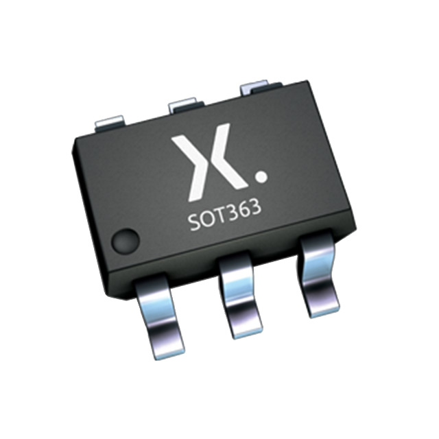
74LVC1G27GW-Q100H
Manufacturer No:
74LVC1G27GW-Q100H
Manufacturer:
Description:
IC GATE NOR 1CH 3-INP SOT363
Datasheet:
Delivery:


Payment:


In Stock : 9566
Please send RFQ , we will respond immediately.


74LVC1G27GW-Q100H Specifications
-
TypeParameter
-
Package / Case6-TSSOP, SC-88, SOT-363
-
Supplier Device Package6-TSSOP
-
Mounting TypeSurface Mount
-
Operating Temperature-40°C ~ 125°C (TA)
-
Max Propagation Delay @ V, Max CL4.5ns @ 5V, 50pF
-
Input Logic Level - High0.95V ~ 3.4V
-
Input Logic Level - Low0.7V ~ 0.8V
-
Current - Output High, Low32mA, 32mA
-
Current - Quiescent (Max)4 µA
-
Voltage - Supply1.65V ~ 5.5V
-
Features-
-
Number of Inputs3
-
Number of Circuits1
-
Logic TypeNOR Gate
-
PackagingCut Tape (CT)
-
PackagingTape & Reel (TR)
-
Product StatusActive
-
SeriesAutomotive, AEC-Q100, 74LVC
The 74LVC1G27GW-Q100H is a single buffer/driver with open-drain output integrated circuit chip. Some of the advantages and application scenarios of this chip are as follows:Advantages: 1. Wide operating voltage range: The chip can operate within a wide voltage range, typically from 1.65V to 5.5V. This makes it suitable for various low-voltage applications. 2. High-speed operation: The chip has a high-speed operation capability, making it suitable for applications that require fast switching and data transmission. 3. Low power consumption: The chip is designed to consume low power, making it suitable for battery-powered devices and energy-efficient applications. 4. Open-drain output: The chip has an open-drain output configuration, which allows for easy interfacing with other devices and enables wired-OR connections.Application Scenarios: 1. Level shifting: The chip can be used for level shifting applications, where it converts signals from one voltage level to another. This is useful when interfacing between devices with different voltage levels. 2. Bus buffering: The chip can be used to buffer and drive signals on a bus, ensuring proper signal integrity and preventing signal degradation. 3. I2C and SMBus applications: The chip can be used in I2C (Inter-Integrated Circuit) and SMBus (System Management Bus) applications, where it can act as a buffer or level shifter for the data and clock lines. 4. GPIO expansion: The chip can be used to expand the number of general-purpose input/output (GPIO) pins of a microcontroller or other digital devices, allowing for more interfacing options. 5. Wired-OR connections: The open-drain output configuration of the chip makes it suitable for wired-OR connections, where multiple devices can share a common signal line and pull it low when needed.These are just a few examples of the advantages and application scenarios of the 74LVC1G27GW-Q100H integrated circuit chip. The specific usage will depend on the requirements of the particular electronic system or project.
74LVC1G27GW-Q100H Relevant information


