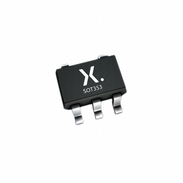
74LVC1G08GW,125
Manufacturer No:
74LVC1G08GW,125
Manufacturer:
Description:
IC GATE AND 1CH 2-INP 5TSSOP
Datasheet:
Delivery:


Payment:


In Stock : 144250
Please send RFQ , we will respond immediately.


74LVC1G08GW,125 Specifications
-
TypeParameter
-
Package / Case5-TSSOP, SC-70-5, SOT-353
-
Supplier Device Package5-TSSOP
-
Mounting TypeSurface Mount
-
Operating Temperature-40°C ~ 125°C (TA)
-
Max Propagation Delay @ V, Max CL4ns @ 5V, 50pF
-
Input Logic Level - High1.7V ~ 2V
-
Input Logic Level - Low0.7V ~ 0.8V
-
Current - Output High, Low32mA, 32mA
-
Current - Quiescent (Max)4 µA
-
Voltage - Supply1.65V ~ 5.5V
-
Features-
-
Number of Inputs2
-
Number of Circuits1
-
Logic TypeAND Gate
-
PackagingCut Tape (CT)
-
PackagingTape & Reel (TR)
-
Product StatusActive
-
Series74LVC
The 74LVC1G08GW,125 is a single-gate AND gate integrated circuit chip. It is part of the 74LVC series of low voltage CMOS (complementary metal-oxide-semiconductor) logic chips. Here are some advantages and application scenarios of the 74LVC1G08GW,125:Advantages: 1. Low power consumption: The 74LVC series is designed for low power applications, making it suitable for battery-powered devices or situations where power efficiency is crucial. 2. Wide operating voltage range: The chip can operate over a wide range of voltages, typically from 1.65V to 5.5V, making it compatible with various power supply levels. 3. Fast switching speed: The 74LVC1G08GW,125 offers high-speed operation, allowing for quick signal processing and response times. 4. Schmitt-trigger input: The chip features a Schmitt-trigger input, which provides hysteresis and enhances the noise immunity and signal shaping capabilities of the chip.Application Scenarios: 1. Logic gate interface: The 74LVC1G08GW,125 can be used as a basic building block for logic gates in digital circuits, such as AND gates, XOR gates, or combinational logic circuits. 2. Signal amplification and buffering: It can be utilized to buffer or amplify digital signals, ensuring robust signal transmission between different parts of a circuit. 3. Interface level shifting: The chip can be employed for level shifting applications, where it converts logic signals from one voltage level to another, enabling compatibility between components or subsystems operating at different voltage levels. 4. Voltage level detection: By utilizing the Schmitt-trigger input, it can be employed for voltage level detection or signal conditioning, where clean and stable signals are critical for accurate operation.These are just some of the advantages and application scenarios of the 74LVC1G08GW,125. However, the specific use cases may vary based on the requirements and design of the electronic system or circuit in which it is integrated.
74LVC1G08GW,125 Relevant information


