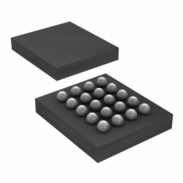
SN74LV374AZQNR
Manufacturer No:
SN74LV374AZQNR
Manufacturer:
Description:
IC FF D-TYPE SNGL 8BIT 20BGA
Datasheet:
Delivery:


Payment:


In Stock : 0
Please send RFQ , we will respond immediately.


SN74LV374AZQNR Specifications
-
TypeParameter
-
Package / Case20-VFBGA
-
Supplier Device Package20-BGA MICROSTAR JUNIOR (4x3)
-
Mounting TypeSurface Mount
-
Operating Temperature-40°C ~ 85°C (TA)
-
Input Capacitance2.9 pF
-
Current - Quiescent (Iq)20 µA
-
Voltage - Supply2V ~ 5.5V
-
Current - Output High, Low16mA, 16mA
-
Trigger TypePositive Edge
-
Max Propagation Delay @ V, Max CL10.1ns @ 5V, 50pF
-
Clock Frequency170 MHz
-
Number of Bits per Element8
-
Number of Elements1
-
Output TypeTri-State, Non-Inverted
-
TypeD-Type
-
FunctionStandard
-
PackagingTape & Reel (TR)
-
Product StatusObsolete
-
Series74LV
The SN74LV374AZQNR is an integrated circuit chip belonging to the 74LV family of devices. It is an octal D-type flip-flop with a 3-state output. Here are some advantages and application scenarios of the SN74LV374AZQNR:Advantages: 1. Low-voltage operation: The "LV" in the part number signifies that the chip operates at low voltages, typically ranging from 2V to 5.5V. This makes it suitable for various applications, including battery-powered devices.2. High-speed operation: The chip has a high-speed toggle flip-flop design, ensuring quick and efficient operation.3. 3-state outputs: The 3-state outputs allow the chip to be used in bus-oriented systems, where multiple devices can share a common bus without interfering with each other.4. Low power consumption: The SN74LV374AZQNR is designed to minimize power consumption, making it energy-efficient.Application scenarios: 1. Data storage and transfer: The flip-flop nature of the chip allows it to store and transfer data efficiently. It can be used in applications where data needs to be latched, such as in registers and memory systems.2. Address decoding: The chip's 3-state outputs are useful in address decoding circuits, where multiple devices share a common bus. It enables the selection of specific devices on the bus and prevents data collision.3. Control signal generation: The octal design of the chip makes it suitable for generating control signals in systems where multiple signals need to be synchronized and controlled.4. Clock signal division: The flip-flop design of the chip allows it to divide a clock signal by 2, making it useful in clocking and timing applications.Overall, the SN74LV374AZQNR is a versatile chip that can be employed in various digital circuits that require low voltage, high speed, low power consumption, and control signal generation.
SN74LV374AZQNR Relevant information


