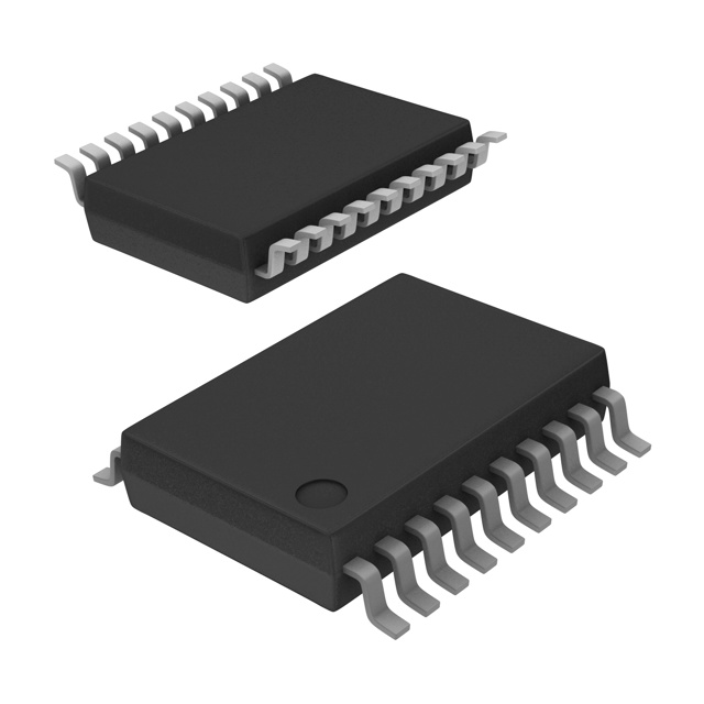
SN74ACT534DBRE4
Manufacturer No:
SN74ACT534DBRE4
Manufacturer:
Description:
IC FF D-TYPE SNGL 8BIT 20SSOP
Datasheet:
Delivery:


Payment:


In Stock : 0
Please send RFQ , we will respond immediately.


SN74ACT534DBRE4 Specifications
-
TypeParameter
-
Package / Case20-SSOP (0.209", 5.30mm Width)
-
Supplier Device Package20-SSOP
-
Mounting TypeSurface Mount
-
Operating Temperature-40°C ~ 85°C (TA)
-
Input Capacitance4.5 pF
-
Current - Quiescent (Iq)4 µA
-
Voltage - Supply4.5V ~ 5.5V
-
Current - Output High, Low24mA, 24mA
-
Trigger TypePositive Edge
-
Max Propagation Delay @ V, Max CL11.5ns @ 5V, 50pF
-
Clock Frequency100 MHz
-
Number of Bits per Element8
-
Number of Elements1
-
Output TypeTri-State, Inverted
-
TypeD-Type
-
FunctionStandard
-
PackagingTape & Reel (TR)
-
Product StatusObsolete
-
Series74ACT
The SN74ACT534DBRE4 is an integrated circuit chip that belongs to the ACT family of logic devices. It is a octal, D-type latch with 3-state outputs, meaning it has eight separate latches with eight independent inputs and outputs. Here are some advantages and application scenarios of the SN74ACT534DBRE4:Advantages: 1. High-speed operation: The SN74ACT534DBRE4 operates at high speeds, making it suitable for applications requiring fast data storage and retrieval. 2. 3-state outputs: The 3-state outputs allow the chip to drive bus lines without the need for external bus drivers, reducing the complexity and cost of a circuit design. 3. Low power consumption: The device is designed to consume low power, making it energy-efficient and suitable for battery-operated devices.Application Scenarios: 1. Data storage and transfer: The 8 latches in the chip can be used to store and transfer data in applications like memory systems, registers, and data buses. 2. Address decoding: The SN74ACT534DBRE4 can be used for address decoding in microprocessors and memory systems, allowing efficient selection of specific memory locations or input/output devices. 3. Bus interface: The 3-state outputs of the chip make it suitable for interfacing with external circuitry, such as connecting multiple devices to a common bus line. 4. FPGA and ASIC designs: The SN74ACT534DBRE4 can be used as a building block in Field Programmable Gate Arrays (FPGAs) or Application Specific Integrated Circuits (ASICs) for various digital logic and control applications. 5. Clock gating: The latch functionality of the chip can be utilized to implement clock gating techniques, where specific parts of a circuit are disabled when not required, reducing power consumption.Overall, the advantages and application scenarios of the SN74ACT534DBRE4 integrated circuit chip make it suitable for a wide range of digital logic applications, including data storage, transfer, bus interfacing, and address decoding.
SN74ACT534DBRE4 Relevant information


