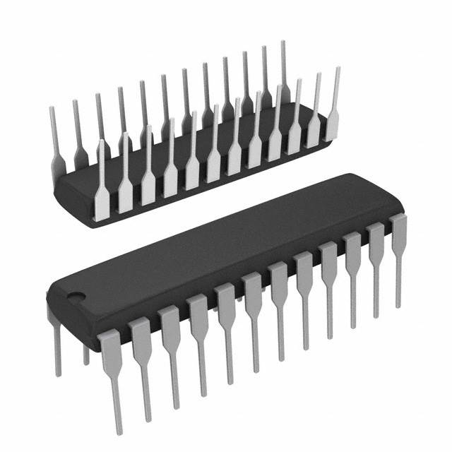
SN74BCT29825NT
Manufacturer No:
SN74BCT29825NT
Manufacturer:
Description:
IC FF D-TYPE SNGL 8BIT 24DIP
Datasheet:
Delivery:


Payment:


In Stock : 0
Please send RFQ , we will respond immediately.


SN74BCT29825NT Specifications
-
TypeParameter
-
Input Capacitance5 pF
-
Clock Frequency125 MHz
-
Package / Case24-DIP (0.300", 7.62mm)
-
Supplier Device Package24-PDIP
-
Mounting TypeThrough Hole
-
Operating Temperature0°C ~ 70°C (TA)
-
Current - Quiescent (Iq)16 mA
-
Voltage - Supply4.5V ~ 5.5V
-
Current - Output High, Low24mA, 48mA
-
Trigger TypePositive Edge
-
Max Propagation Delay @ V, Max CL7.8ns @ 5V, 50pF
-
Number of Bits per Element8
-
Number of Elements1
-
Output TypeTri-State, Non-Inverted
-
TypeD-Type
-
FunctionMaster Reset
-
PackagingTube
-
PackagingTube
-
Product StatusObsolete
-
Series74BCT
The SN74BCT29825NT is a quad universal two-input multiplexer and latches with 3-state outputs integrated circuit chip. Some of the advantages and application scenarios of the SN74BCT29825NT chip are as follows:Advantages: 1. Versatility: The chip features four universal two-input multiplexers, which allows for flexible data selection and routing capabilities. 2. 3-state outputs: The 3-state outputs enable the chip to effectively interface with multiple devices, allowing for efficient control and communication. 3. Latch functionality: The chip also includes latch functionality, which can store and retain data, improving overall performance and reliability. 4. Compatibility: The SN74BCT29825NT is compatible with both TTL and CMOS logic, ensuring easy integration into various digital systems. 5. High speed: The chip operates at high speeds, making it suitable for applications where quick data processing and transmission are crucial. 6. Low power consumption: The chip consumes minimal power, resulting in energy efficiency and reduced heat generation.Application scenarios: 1. Data routing and selection: The multiplexer functionality of the chip makes it applicable in scenarios where data needs to be selected from multiple sources and routed to different destinations. 2. Data storage: The latch feature allows the chip to store and retain data, making it useful in applications requiring temporary data storage or data buffering. 3. Control systems: The 3-state outputs enable the chip to interface with control systems, such as microcontrollers, I/O expanders, or memory devices, allowing for efficient control and communication. 4. Digital communication systems: The high speed and compatibility with different logic families make the chip suitable for use in digital communication systems, such as serial data transmission, parallel data processing, or bus interfaces. 5. Embedded systems: The versatility and low power consumption of the chip make it applicable in various embedded systems, such as consumer electronics, industrial automation, or automotive electronics, where space and power efficiency are critical.It's important to note that the specific application scenarios may vary depending on the requirements and design of the overall system.
SN74BCT29825NT Relevant information


