


Share

74LVCH162374ADGG:5
Manufacturer No:
74LVCH162374ADGG:5
Manufacturer:
Description:
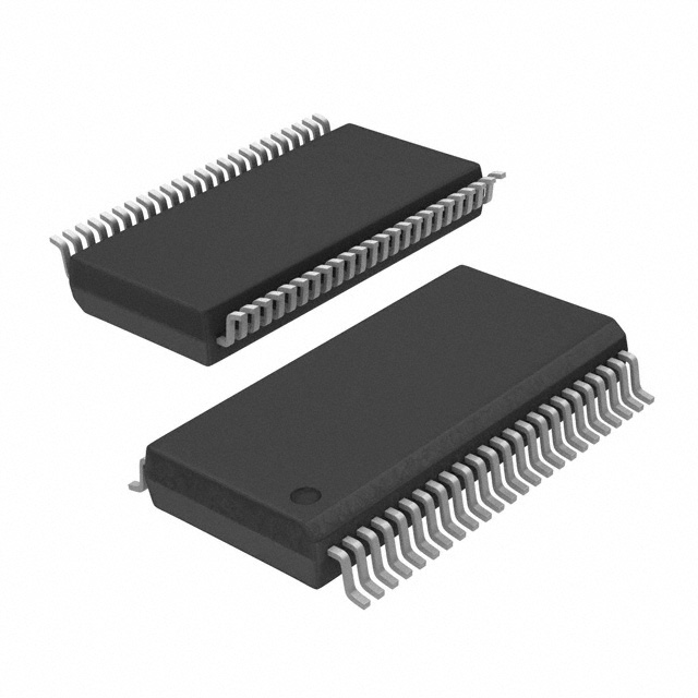
IC FF D-TYPE DUAL 8BIT 48TSSOP
Datasheet:
Delivery:


Payment:


In Stock : 0
Please send RFQ , we will respond immediately.


74LVCH162374ADGG:5 Specifications
-
TypeParameter
-
Package / Case48-TFSOP (0.240", 6.10mm Width)
-
Supplier Device Package48-TSSOP
-
Mounting TypeSurface Mount
-
Operating Temperature-40°C ~ 125°C (TA)
-
Input Capacitance5 pF
-
Current - Quiescent (Iq)20 µA
-
Voltage - Supply1.65V ~ 3.6V
-
Current - Output High, Low12mA, 12mA
-
Trigger TypePositive Edge
-
Max Propagation Delay @ V, Max CL6.8ns @ 3.3V, 50pF
-
Clock Frequency330 MHz
-
Number of Bits per Element8
-
Number of Elements2
-
Output TypeTri-State, Non-Inverted
-
TypeD-Type
-
FunctionStandard
-
PackagingTape & Reel (TR)
-
Product StatusObsolete
-
Series74LVCH
The 74LVCH162374ADGG:5 is a specific type of integrated circuit chip that belongs to the 74LVCH family. It is a 16-bit edge-triggered D-type flip-flop with 3-state outputs. Here are some advantages and application scenarios of this chip:Advantages: 1. High-speed operation: The 74LVCH162374ADGG:5 chip operates at a high speed, making it suitable for applications that require fast data transfer and processing. 2. Low power consumption: This chip is designed to consume low power, making it energy-efficient and suitable for battery-powered devices. 3. 3-state outputs: The chip has 3-state outputs, which means it can be set to high impedance state, allowing multiple chips to be connected to a common bus without causing conflicts. 4. Edge-triggered flip-flop: The chip uses edge-triggered D-type flip-flops, which ensures reliable and synchronized data storage and transfer.Application scenarios: 1. Data storage and transfer: The 74LVCH162374ADGG:5 chip can be used in applications where data needs to be stored and transferred between different components or subsystems. It can be used in data buses, memory systems, and communication interfaces. 2. Address and control signal buffering: The chip can be used to buffer address and control signals in microprocessors and digital systems, ensuring proper signal integrity and preventing signal degradation. 3. Bus interfacing: The 3-state outputs of the chip make it suitable for bus interfacing applications, where multiple devices need to share a common bus without causing conflicts or data corruption. 4. Clock signal distribution: The chip can be used to distribute clock signals in synchronous digital systems, ensuring synchronized operation of various components. 5. FPGA and ASIC designs: The 74LVCH162374ADGG:5 chip can be used in Field-Programmable Gate Array (FPGA) and Application-Specific Integrated Circuit (ASIC) designs, where it can serve as a building block for various digital logic functions.It is important to note that the specific advantages and application scenarios may vary depending on the overall system requirements and design considerations.
74LVCH162374ADGG:5 Relevant information