


Share

SN74AC374DBR
Manufacturer No:
SN74AC374DBR
Manufacturer:
Description:
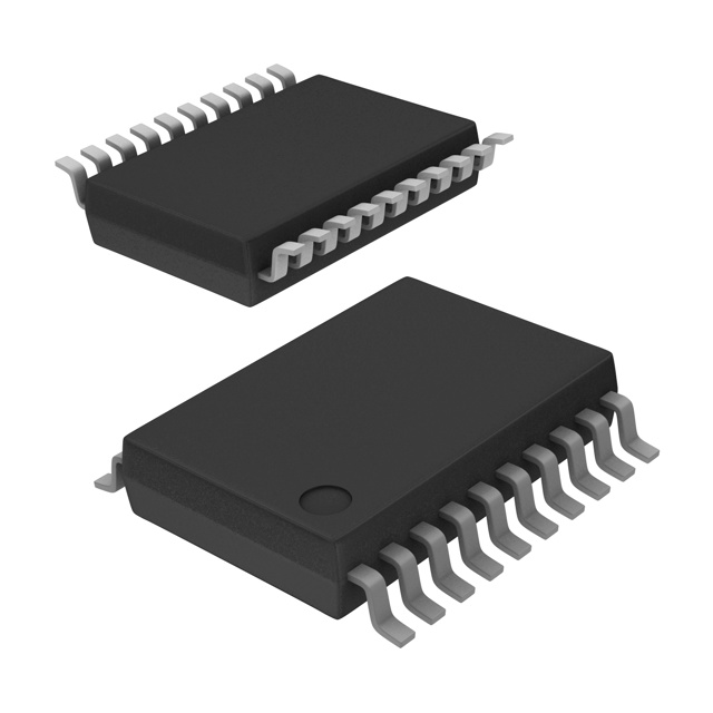
IC FF D-TYPE SNGL 8BIT 20SSOP
Datasheet:
Delivery:


Payment:


In Stock : 0
Please send RFQ , we will respond immediately.


SN74AC374DBR Specifications
-
TypeParameter
-
Package / Case20-SSOP (0.209", 5.30mm Width)
-
Supplier Device Package20-SSOP
-
Mounting TypeSurface Mount
-
Operating Temperature-40°C ~ 85°C (TA)
-
Input Capacitance4.5 pF
-
Current - Quiescent (Iq)4 µA
-
Voltage - Supply2V ~ 6V
-
Current - Output High, Low24mA, 24mA
-
Trigger TypePositive Edge
-
Max Propagation Delay @ V, Max CL9.5ns @ 5V, 50pF
-
Clock Frequency155 MHz
-
Number of Bits per Element8
-
Number of Elements1
-
Output TypeTri-State, Non-Inverted
-
TypeD-Type
-
FunctionStandard
-
PackagingCut Tape (CT)
-
PackagingTape & Reel (TR)
-
Product StatusActive
-
Series74AC
The SN74AC374DBR is a octal edge-triggered D-type flip-flop integrated circuit chip manufactured by Texas Instruments. It offers several advantages and can be used in various application scenarios, including:1. High-speed operation: The SN74AC374DBR chip operates at a high-speed range, making it suitable for applications that require fast data transfer and processing.2. Edge-triggered design: The chip utilizes an edge-triggered design, which means that the output changes only when a rising or falling edge is detected on the clock input. This makes it ideal for applications that require synchronized data transfer and timing control.3. 3-state outputs: The chip features 3-state outputs, allowing multiple chips to be connected to a common bus without conflicts. This enables efficient data sharing and multiplexing in applications such as address decoding and data transfer between buses.4. Wide operating voltage range: The chip operates within a wide voltage range from 2V to 6V, providing flexibility in various power supply setups.5. Low power consumption: The SN74AC374DBR chip is designed to consume low power, making it suitable for battery-powered devices or applications where power efficiency is crucial.Application scenarios where the SN74AC374DBR chip can be used include:1. Data storage and transfer: The chip can be used for data storage in registers, buffers, or shift registers. It allows synchronous transfer of data between different stages of a circuit, ensuring accurate and reliable data handling.2. Address decoding: With its 3-state outputs, the chip can be used in address decoding circuits where multiple devices need access to a shared bus. It enables efficient communication and eliminates conflicts during data transfer on the bus.3. Control and timing circuits: The edge-triggered design of the chip makes it suitable for control and timing applications such as clock synchronization, state control, and sequencing in digital circuits.4. Data multiplexing: By utilizing the 3-state outputs, the chip can serve as a multiplexer, allowing multiple data inputs to be selected and routed to a single output. This is particularly useful in applications involving data selection and routing, such as in communication systems or data routing networks.Overall, the SN74AC374DBR chip offers high-speed operation, edge-triggered design, 3-state outputs, wide voltage range, and low power consumption. These features make it a versatile choice for various applications requiring synchronized data transfer, address decoding, control and timing, and data multiplexing.
SN74AC374DBR Relevant information