


Share

SN74LVC374ADGVR
Manufacturer No:
SN74LVC374ADGVR
Manufacturer:
Description:
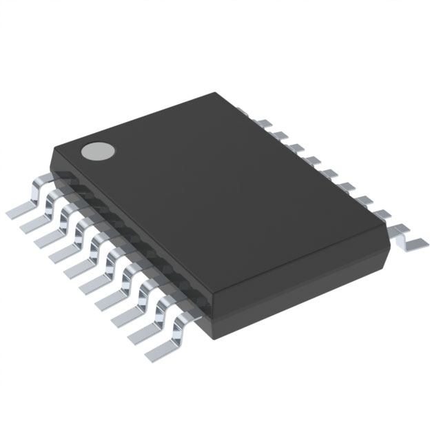
IC FF D-TYPE SNGL 8BIT 20TVSOP
Datasheet:
Delivery:


Payment:


In Stock : 0
Please send RFQ , we will respond immediately.


SN74LVC374ADGVR Specifications
-
TypeParameter
-
Package / Case20-TFSOP (0.173", 4.40mm Width)
-
Supplier Device Package20-TVSOP
-
Mounting TypeSurface Mount
-
Operating Temperature-40°C ~ 85°C (TA)
-
Input Capacitance4 pF
-
Current - Quiescent (Iq)10 µA
-
Voltage - Supply1.65V ~ 3.6V
-
Current - Output High, Low24mA, 24mA
-
Trigger TypePositive Edge
-
Max Propagation Delay @ V, Max CL7ns @ 3.3V, 50pF
-
Clock Frequency100 MHz
-
Number of Bits per Element8
-
Number of Elements1
-
Output TypeTri-State, Non-Inverted
-
TypeD-Type
-
FunctionStandard
-
PackagingCut Tape (CT)
-
PackagingTape & Reel (TR)
-
Product StatusActive
-
Series74LVC
The SN74LVC374ADGVR is an integrated circuit chip that belongs to the LVC family of devices. It is an octal (8-bit) D-type flip-flop with 3-state outputs. Here are some advantages and application scenarios of this chip:Advantages: 1. Low voltage operation: The SN74LVC374ADGVR operates at a voltage range of 1.65V to 5.5V, making it suitable for low power and battery-powered applications. 2. Fast operation: It has a high-speed switching capability with a propagation delay of only 3.5 ns, allowing for efficient data transfer and processing. 3. 3-state outputs: The chip has 3-state outputs, which means the outputs can be independently enabled or disabled, allowing multiple devices to share a common bus. 4. Low power consumption: It has a low power consumption feature due to its LVC family design, making it ideal for portable and battery-powered devices.Application Scenarios: 1. Data storage and buffering: The SN74LVC374ADGVR can be used to store and manipulate data in various applications like microcontrollers, memory interfacing, and data buffering. 2. Bus interface and level conversion: It can be used as a level translator for interfacing different voltage level devices on a common bus, ensuring compatibility between devices operating at different voltage levels. 3. Clock and delay circuits: The chip can be used to design clock generators and delay circuits used in various digital systems like microprocessors, FPGAs, and communication devices. 4. Parallel-to-serial and serial-to-parallel conversion: This chip can be utilized in systems that require conversion between parallel and serial data formats, such as serial communication protocols and data transmission applications. 5. Address decoding and multiplexing: It can be used to demultiplex and decode address lines in memory systems to enable and select specific memory locations.Overall, the SN74LVC374ADGVR integrated circuit chip offers advantages such as low voltage operation, fast switching, 3-state outputs, and low power consumption, making it suitable for a wide range of applications across different industries.
SN74LVC374ADGVR Relevant information