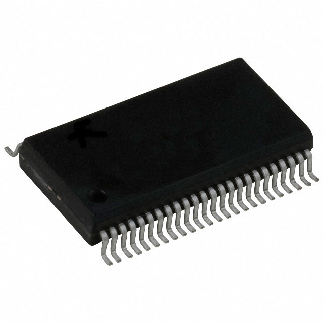
SN74LVTH162374DGGR
Manufacturer No:
SN74LVTH162374DGGR
Manufacturer:
Description:
IC FF D-TYPE DUAL 8BIT 48TSSOP
Datasheet:
Delivery:


Payment:


In Stock : 224
Please send RFQ , we will respond immediately.


SN74LVTH162374DGGR Specifications
-
TypeParameter
-
Package / Case48-TFSOP (0.240", 6.10mm Width)
-
Supplier Device Package48-TSSOP
-
Mounting TypeSurface Mount
-
Operating Temperature-40°C ~ 85°C (TA)
-
Input Capacitance3 pF
-
Current - Quiescent (Iq)190 µA
-
Voltage - Supply2.7V ~ 3.6V
-
Current - Output High, Low12mA, 12mA
-
Trigger TypePositive Edge
-
Max Propagation Delay @ V, Max CL5.3ns @ 3.3V, 50pF
-
Clock Frequency160 MHz
-
Number of Bits per Element8
-
Number of Elements2
-
Output TypeTri-State, Non-Inverted
-
TypeD-Type
-
FunctionStandard
-
PackagingCut Tape (CT)
-
PackagingTape & Reel (TR)
-
Product StatusActive
-
Series74LVTH
The SN74LVTH162374DGGR is a 16-bit edge-triggered D-type flip-flop with 3-state outputs. Here are some advantages and application scenarios of this integrated circuit chip:Advantages: 1. High-speed operation: The LVTH series is designed for high-speed applications, making it suitable for use in systems that require fast data transfer. 2. Low power consumption: The LVTH series is designed to operate at low power, making it energy-efficient and suitable for battery-powered devices. 3. 3-state outputs: The 3-state outputs allow multiple devices to share a common bus, enabling efficient data transfer and reducing the number of required pins. 4. Edge-triggered flip-flops: The edge-triggered design ensures that the outputs change only on the rising or falling edge of the clock signal, providing precise control over data transfer.Application scenarios: 1. Data storage and transfer: The flip-flops in this chip can be used to store and transfer data in various digital systems, such as microprocessors, memory modules, and communication interfaces. 2. Bus interfacing: The 3-state outputs make this chip suitable for bus interfacing applications, where multiple devices need to share a common data bus. 3. Clock synchronization: The edge-triggered flip-flops can be used to synchronize data with a clock signal, ensuring accurate and reliable data transfer in synchronous systems. 4. Address decoding: The chip can be used in address decoding circuits to enable or disable specific memory or peripheral devices based on the address signals.Overall, the SN74LVTH162374DGGR integrated circuit chip offers high-speed operation, low power consumption, 3-state outputs, and edge-triggered flip-flops, making it suitable for various applications involving data storage, transfer, bus interfacing, clock synchronization, and address decoding.
SN74LVTH162374DGGR Relevant information


