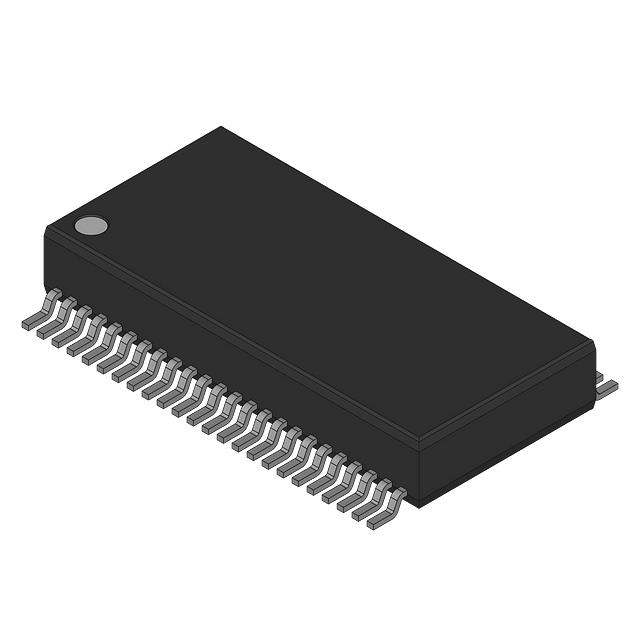
CY74FCT16374ATPVC
Manufacturer No:
CY74FCT16374ATPVC
Manufacturer:
Description:
IC FF D-TYPE DUAL 8BIT 48SSOP
Datasheet:
Delivery:


Payment:


In Stock : 581
Please send RFQ , we will respond immediately.


CY74FCT16374ATPVC Specifications
-
TypeParameter
-
Package / Case48-BSSOP (0.295", 7.50mm Width)
-
Supplier Device Package48-SSOP
-
Mounting TypeSurface Mount
-
Operating Temperature-40°C ~ 85°C (TA)
-
Input Capacitance4.5 pF
-
Current - Quiescent (Iq)500 µA
-
Voltage - Supply4.5V ~ 5.5V
-
Current - Output High, Low32mA, 64mA
-
Trigger TypePositive Edge
-
Max Propagation Delay @ V, Max CL-
-
Number of Bits per Element8
-
Number of Elements2
-
Output TypeTri-State, Non-Inverted
-
TypeD-Type
-
FunctionStandard
-
PackagingBulk
-
Product StatusActive
-
Series74FCT
The CY74FCT16374ATPVC is a 16-bit edge-triggered D-type flip-flop integrated circuit chip. It offers several advantages and can be used in various application scenarios:Advantages: 1. High-speed operation: The CY74FCT16374ATPVC chip operates at a high-speed clock frequency, making it suitable for applications that require fast data transfer and processing. 2. Low power consumption: It is designed to consume low power, making it energy-efficient and suitable for battery-powered devices or applications where power efficiency is crucial. 3. Edge-triggered design: The chip is triggered by the rising or falling edge of the clock signal, ensuring reliable and synchronized data transfer. 4. 3-state outputs: The chip has 3-state outputs, allowing multiple devices to be connected to a common bus without conflicts or contention. 5. Wide operating voltage range: It can operate within a wide voltage range, making it compatible with various voltage levels commonly used in digital systems.Application scenarios: 1. Data storage and transfer: The CY74FCT16374ATPVC chip can be used in applications where data needs to be stored and transferred, such as memory systems, registers, and data buses. 2. Synchronous data processing: It is suitable for applications that require synchronized data processing, such as digital signal processing, data communication systems, and microprocessors. 3. Address and control signal buffering: The 3-state outputs of the chip make it suitable for buffering address and control signals in systems with multiple devices connected to a common bus. 4. Clock signal synchronization: It can be used to synchronize clock signals in systems with multiple clock domains, ensuring proper timing and avoiding data corruption. 5. Industrial automation and control systems: The high-speed operation and low power consumption of the chip make it suitable for use in industrial automation and control systems, where fast and efficient data processing is required.Overall, the CY74FCT16374ATPVC chip offers advantages such as high-speed operation, low power consumption, and edge-triggered design, making it suitable for various applications that involve data storage, transfer, synchronization, and control.
CY74FCT16374ATPVC Relevant information


