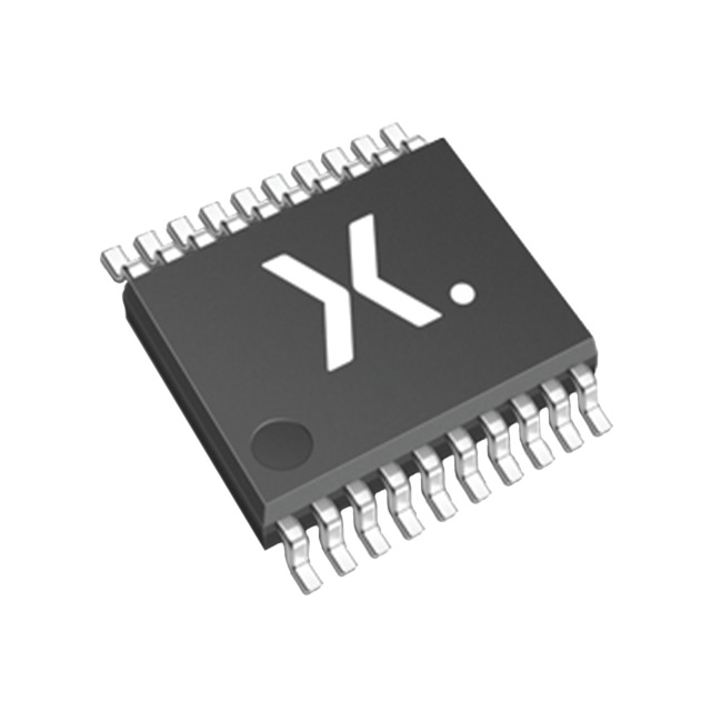
74HC273PW-Q100J
Manufacturer No:
74HC273PW-Q100J
Manufacturer:
Description:
IC FF D-TYPE SNGL 8BIT 20TSSOP
Datasheet:
Delivery:


Payment:


In Stock : 2495
Please send RFQ , we will respond immediately.


74HC273PW-Q100J Specifications
-
TypeParameter
-
Clock Frequency122 MHz
-
Package / Case20-TSSOP (0.173", 4.40mm Width)
-
Supplier Device Package20-TSSOP
-
Mounting TypeSurface Mount
-
Operating Temperature-40°C ~ 125°C (TA)
-
Input Capacitance3.5 pF
-
Current - Quiescent (Iq)8 µA
-
Voltage - Supply2V ~ 6V
-
Current - Output High, Low5.2mA, 5.2mA
-
Trigger TypePositive Edge
-
Max Propagation Delay @ V, Max CL26ns @ 6V, 50pF
-
Number of Bits per Element8
-
Number of Elements1
-
Output TypeNon-Inverted
-
TypeD-Type
-
FunctionMaster Reset
-
PackagingCut Tape (CT)
-
PackagingTape & Reel (TR)
-
Product StatusActive
-
SeriesAutomotive, AEC-Q100, 74HC
The 74HC273PW-Q100J is an octal D-type flip-flop integrated circuit chip. Some advantages and application scenarios of this chip include:1. High-speed operation: The 74HC273PW-Q100J chip is designed for high-speed operation, making it suitable for applications that require fast data storage and retrieval.2. Low power consumption: This chip operates at a low power supply voltage, making it energy-efficient and suitable for battery-powered devices.3. Multiple data input pins: The chip has eight D-type flip-flops with individual data inputs, enabling the storage of multiple data bits simultaneously.4. Edge-triggered flip-flops: The flip-flops in this chip are triggered by the rising or falling edge of the clock signal, providing precise control over data storage.5. Non-inverting outputs: The chip's outputs are non-inverting, meaning they provide the same logic level as the input data.Application scenarios:1. Registers: The 74HC273PW-Q100J chip can be used to implement registers in microcontrollers and digital systems where data needs to be stored temporarily.2. Address decoding: This chip can be used in address decoding circuits, where it helps in interpreting and selecting specific memory or peripheral addresses.3. State machine design: With its multiple flip-flops, the chip can be used to design state machines that require the storage and manipulation of binary states.4. Data synchronization: The chip can be used to synchronize data streams in communication systems, ensuring reliable transmission and reception of data.5. Clock signal division: The chip can divide an input clock signal by two, four, or eight, providing clock signals at slower frequencies for timing purposes.Overall, the 74HC273PW-Q100J chip's high-speed operation, low power consumption, and versatile functionality make it suitable for a wide range of digital circuit designs and applications.
74HC273PW-Q100J Relevant information


