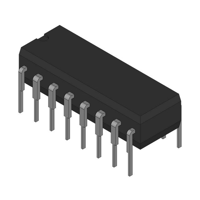
CD74AC112E
Manufacturer No:
CD74AC112E
Manufacturer:
Description:
IC FF JK TYPE DUAL 1BIT 16DIP
Datasheet:
Delivery:


Payment:


In Stock : 20239
Please send RFQ , we will respond immediately.


CD74AC112E Specifications
-
TypeParameter
-
Package / Case16-DIP (0.300", 7.62mm)
-
Supplier Device Package16-PDIP
-
Mounting TypeThrough Hole
-
Operating Temperature-55°C ~ 125°C (TA)
-
Input Capacitance10 pF
-
Current - Quiescent (Iq)4 µA
-
Voltage - Supply1.5V ~ 5.5V
-
Current - Output High, Low24mA, 24mA
-
Trigger TypeNegative Edge
-
Max Propagation Delay @ V, Max CL10.3ns @ 5V, 50pF
-
Clock Frequency100 MHz
-
Number of Bits per Element1
-
Number of Elements2
-
Output TypeComplementary
-
TypeJK Type
-
FunctionSet(Preset) and Reset
-
PackagingTube
-
Product StatusObsolete
-
Series74AC
The CD74AC112E is a dual negative-edge triggered JK flip-flop integrated circuit chip. It has several advantages and application scenarios, including:1. High-speed operation: The CD74AC112E operates at high-speed, making it suitable for applications that require quick response times.2. Low power consumption: This chip has low power consumption, making it energy-efficient and suitable for battery-powered devices.3. Wide operating voltage range: The CD74AC112E can operate within a wide voltage range, typically between 2V and 6V, making it compatible with various power supply configurations.4. Noise immunity: It has a high noise immunity, which means it can tolerate external noise and interference, ensuring reliable operation in noisy environments.5. Dual flip-flop configuration: The CD74AC112E consists of two independent JK flip-flops in a single chip, allowing for compact circuit designs and reducing the number of components required.Application scenarios for the CD74AC112E include:1. Digital logic circuits: It can be used in various digital logic circuits, such as counters, registers, and sequencers, where flip-flops are required for storing and manipulating binary data.2. Control systems: The CD74AC112E can be used in control systems to store and synchronize control signals, enabling precise timing and sequencing of operations.3. Data storage and transfer: It can be used in applications that require temporary storage or transfer of data, such as data buffers, data multiplexers, or data synchronization circuits.4. Clock and timing circuits: The CD74AC112E can be used in clock and timing circuits to generate and synchronize clock signals, enabling precise timing control in various digital systems.5. Communication systems: It can be used in communication systems for data synchronization, error detection, and correction, ensuring reliable data transmission.Overall, the CD74AC112E integrated circuit chip offers high-speed operation, low power consumption, and noise immunity, making it suitable for a wide range of digital logic and control applications.
CD74AC112E Relevant information


