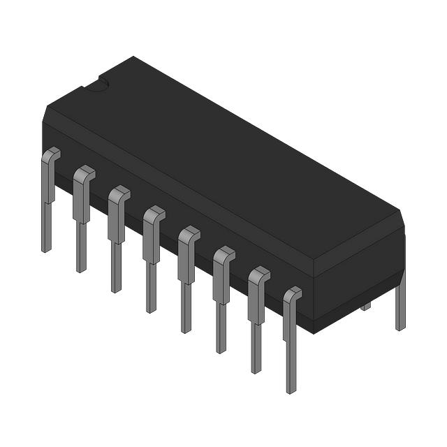
SN74LVC112ANS
Manufacturer No:
SN74LVC112ANS
Manufacturer:
Description:
IC FF JK TYPE DUAL 1BIT 16SO
Datasheet:
Delivery:


Payment:


In Stock : 21150
Please send RFQ , we will respond immediately.


SN74LVC112ANS Specifications
-
TypeParameter
-
Input Capacitance4.5 pF
-
Package / Case16-SOIC (0.209", 5.30mm Width)
-
Supplier Device Package16-SO
-
Mounting TypeSurface Mount
-
Operating Temperature-40°C ~ 85°C (TA)
-
Current - Quiescent (Iq)10 µA
-
Voltage - Supply1.65V ~ 3.6V
-
Current - Output High, Low24mA, 24mA
-
Trigger TypeNegative Edge
-
Max Propagation Delay @ V, Max CL5.9ns @ 3.3V, 50pF
-
Clock Frequency150 MHz
-
Number of Bits per Element1
-
Number of Elements2
-
Output TypeComplementary
-
TypeJK Type
-
FunctionSet(Preset) and Reset
-
PackagingBulk
-
Product StatusActive
-
Series74LVC
The SN74LVC112ANS is a dual negative-edge triggered D-type flip-flop integrated circuit (IC) chip manufactured by Texas Instruments. Some advantages and application scenarios of the SN74LVC112ANS are as follows:Advantages: 1. Low voltage operation: The SN74LVC112ANS is designed to operate at low voltage levels, typically ranging from 1.65V to 3.6V. This makes it suitable for applications where power consumption needs to be minimized, such as in portable devices.2. High-speed operation: With a maximum propagation delay of just 3.4 nanoseconds, the SN74LVC112ANS can handle high-speed data processing and control signals. This makes it suitable for applications that require quick response times.3. Dual flip-flop configuration: The SN74LVC112ANS consists of two individual D-type flip-flops, allowing it to handle two separate data input signals simultaneously. This configuration is useful in applications where multiple sequential data operations need to be synchronized.4. Negative-edge triggered: The flip-flops in the SN74LVC112ANS respond to the falling edge of the clock signal. This feature allows for precise timing and can simplify the design of certain applications.Application Scenarios: 1. Sequential logic circuits: The SN74LVC112ANS can be used in sequential logic circuits to store and manipulate data. It is commonly used in applications such as counters, shift registers, and state machines.2. Data synchronization: The dual flip-flop configuration and precise timing capability of the SN74LVC112ANS make it suitable for applications that require data synchronization. It can be used to prevent data hazards and ensure proper data transfer in digital systems.3. Registers and memory elements: The SN74LVC112ANS can be used as building blocks for various kinds of registers and memory elements, providing data storage and retrieval capabilities. It is often used in microcontrollers, digital signal processors (DSPs), and other memory-intensive applications.4. Clock signal handling: Due to its negative-edge triggered nature, the SN74LVC112ANS can be used to handle clock signals in circuits that require synchronized data processing and control. It allows for precise control of the clock signal and can help avoid timing issues.Overall, the SN74LVC112ANS flip-flop IC chip offers reliable and efficient data manipulation and storage capabilities. Its low voltage operation, high-speed performance, and synchronous functionality make it suitable for a wide range of applications in digital systems.
SN74LVC112ANS Relevant information


