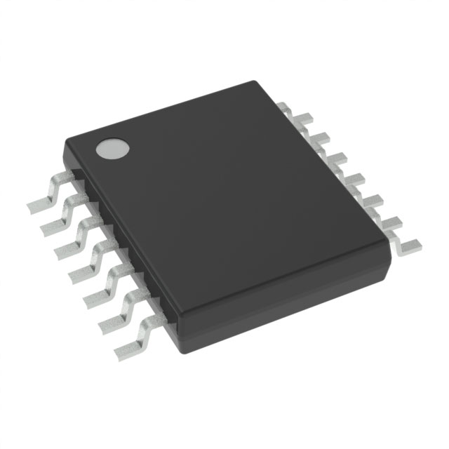
SN74AHCT126QPWREP
Manufacturer No:
SN74AHCT126QPWREP
Manufacturer:
Description:
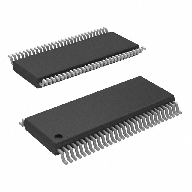
IC BUF NON-INVERT 5.5V 14TSSOP
Datasheet:
Delivery:


Payment:


In Stock : 0
Please send RFQ , we will respond immediately.


SN74AHCT126QPWREP Specifications
-
TypeParameter
-
Supplier Device Package14-TSSOP
-
Package / Case14-TSSOP (0.173", 4.40mm Width)
-
Mounting TypeSurface Mount
-
Operating Temperature-40°C ~ 125°C (TA)
-
Voltage - Supply4.5V ~ 5.5V
-
Current - Output High, Low8mA, 8mA
-
Output Type3-State
-
Input Type-
-
Number of Bits per Element1
-
Number of Elements4
-
Logic TypeBuffer, Non-Inverting
-
PackagingCut Tape (CT)
-
PackagingTape & Reel (TR)
-
Product StatusActive
-
Series74AHCT
The SN74AHCT126QPWREP is a specific variant of the SN74AHCT126QPWREP integrated circuit chip series, which is a quad bus buffer gate with three-state outputs. Some advantages and application scenarios of this chip include:Advantages: 1. High-Speed Operation: The SN74AHCT126Q series is designed to operate at high clock frequencies, making it suitable for applications that require fast data transfers and signal processing. 2. Compatibility: The chip is compatible with TTL, CMOS, and HCT logic families, allowing for easy integration into existing circuit designs. 3. Three-State Outputs: The three-state outputs enable the chip to directly interface with a bus, enabling multiple devices to share and control a common data line. 4. Low Power Consumption: The AHCT series offers low power consumption, making it favorable for portable and energy-efficient devices. 5. Flexible Supply Voltage Range: The chip can operate with a wide supply voltage range, typically from 4.5V to 5.5V, allowing for compatibility with various power sources.Application Scenarios: 1. Data Bus Buffering: The SN74AHCT126QPWREP chip can be used to buffer and control data signals in multi-device systems where several components share a common bus. 2. Level Shifting: It can be utilized for level shifting applications to convert signals between different logic families, such as converting a TTL signal to a CMOS compatible signal. 3. Clock Signal Distribution: The chip can distribute clock signals in synchronous systems, maintaining signal integrity and minimizing clock skew. 4. Memory Systems: In memory systems, the chip can be used to control the read and write operations, ensuring reliable and simultaneous data access. 5. I/O Expansion: The SN74AHCT126QPWREP chip can expand the number of input/output pins of a microcontroller or microprocessor, allowing for increased connectivity and peripheral control.It's worth noting that specific application scenarios may vary based on the requirements of the circuit design and system configuration.
SN74AHCT126QPWREP Relevant information
-

SN74ALVTH162245LR
Texas Instruments -
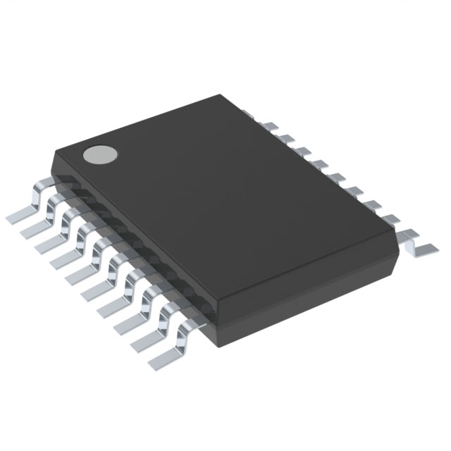
SN74BCT623NSR
Texas Instruments -
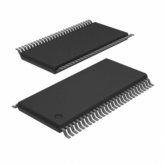
CY74FCT16543ATPACT
Texas Instruments -
SN74LVTH652DGVR
Texas Instruments -
SN74LVTH646DGVR
Texas Instruments -
SN74LVTH2952DGVR
Texas Instruments -

SN74LVTH162241DL
Texas Instruments -
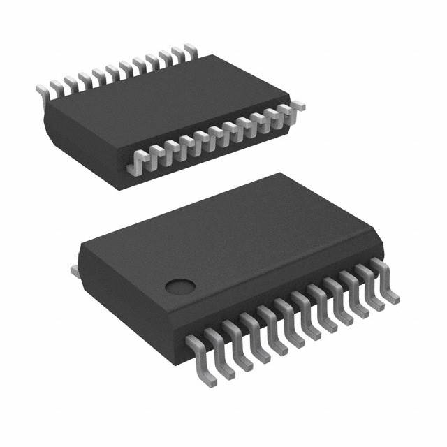
SN74LVC828ADBR
Texas Instruments -

SN74ALVTH162244LR
Texas Instruments -
SN74ALVCH162344VR
Texas Instruments


