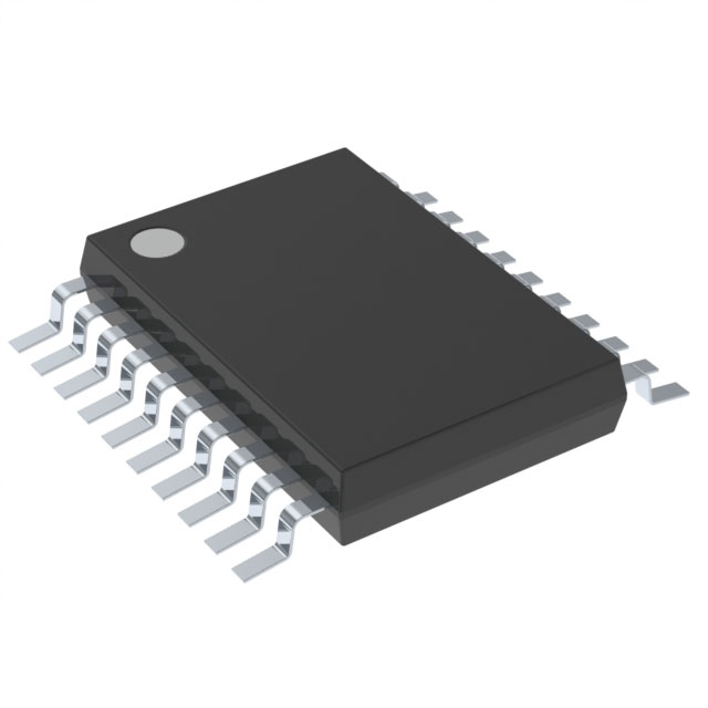
74LVC2G240DC-Q100H
Manufacturer No:
74LVC2G240DC-Q100H
Manufacturer:
Description:
IC BUFFER INVERT 5.5V 8VSSOP
Datasheet:
Delivery:


Payment:


In Stock : 0
Please send RFQ , we will respond immediately.


74LVC2G240DC-Q100H Specifications
-
TypeParameter
-
Supplier Device Package8-VSSOP
-
Package / Case8-VFSOP (0.091", 2.30mm Width)
-
Mounting TypeSurface Mount
-
Operating Temperature-40°C ~ 125°C (TA)
-
Voltage - Supply1.65V ~ 5.5V
-
Current - Output High, Low32mA, 32mA
-
Output Type3-State
-
Input Type-
-
Number of Bits per Element1
-
Number of Elements2
-
Logic TypeBuffer, Inverting
-
PackagingCut Tape (CT)
-
PackagingTape & Reel (TR)
-
Product StatusActive
-
SeriesAutomotive, AEC-Q100, 74LVC
The 74LVC2G240DC-Q100H is a dual non-inverting buffer/line driver integrated circuit chip. It belongs to the LVC family, which is a part of the CMOS logic family. Here are some advantages and application scenarios of the 74LVC2G240DC-Q100H:Advantages: 1. Low voltage operation: The chip supports voltage levels from 1.65V to 5.5V, making it suitable for both low-power and high-power applications. 2. Fast switching speed: It provides high-speed switching, allowing for quick data transmission and signal amplification. 3. Low power consumption: The chip is designed to consume minimal power, making it energy-efficient and suitable for battery-operated devices. 4. Schmitt-trigger input: It includes input Schmitt triggers that help in achieving reliable and noise-tolerant signal processing. 5. Triple-balanced outputs: It offers symmetrical output impedance, making it suitable for driving both resistive and capacitive loads.Application scenarios: 1. Voltage level translation: The 74LVC2G240DC-Q100H can be used to convert logic levels between different voltage domains, enabling communication between circuits operating at different voltage levels. 2. Signal buffering: It is often used to buffer and amplify signals in various systems, preventing signal degradation and maintaining signal integrity. 3. Standard logic gate replacement: The chip can be used as a drop-in replacement for standard logic gates, offering improved performance and lower power consumption. 4. Input/output expansion: It is commonly used to expand the number of inputs or outputs in microcontrollers, FPGAs, and other digital systems. 5. Interface protection: The chip can be used to protect sensitive components from voltage spikes or noise by buffering and isolating the signals.These are just a few of the advantages and application scenarios of the 74LVC2G240DC-Q100H chip. Its versatility and features make it suitable for a wide range of digital logic and signal processing applications.
74LVC2G240DC-Q100H Relevant information
-

SN74ALVTH162245LR
Texas Instruments -

SN74BCT623NSR
Texas Instruments -

CY74FCT16543ATPACT
Texas Instruments -
SN74LVTH652DGVR
Texas Instruments -
SN74LVTH646DGVR
Texas Instruments -
SN74LVTH2952DGVR
Texas Instruments -

SN74LVTH162241DL
Texas Instruments -

SN74LVC828ADBR
Texas Instruments -

SN74ALVTH162244LR
Texas Instruments -

SN74ALVCH162344VR
Texas Instruments


