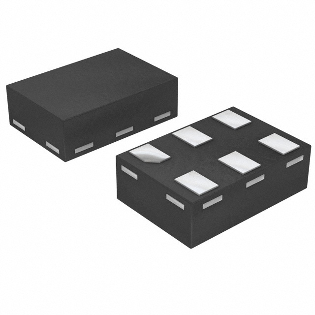
74AUP1G34FW5-7
Manufacturer No:
74AUP1G34FW5-7
Manufacturer:
Description:
IC BUFFER NON-INVERT 3.6V 6DFN
Datasheet:
Delivery:


Payment:


In Stock : 0
Please send RFQ , we will respond immediately.


74AUP1G34FW5-7 Specifications
-
TypeParameter
-
Supplier Device PackageX1-DFN1010-6
-
Package / Case6-XFDFN
-
Mounting TypeSurface Mount
-
Operating Temperature-40°C ~ 125°C (TA)
-
Voltage - Supply0.8V ~ 3.6V
-
Current - Output High, Low4mA, 4mA
-
Output TypePush-Pull
-
Input Type-
-
Number of Bits per Element1
-
Number of Elements1
-
Logic TypeBuffer, Non-Inverting
-
PackagingCut Tape (CT)
-
PackagingTape & Reel (TR)
-
Product StatusActive
-
Series74AUP
The 74AUP1G34FW5-7 is a single buffer gate integrated circuit chip with open-drain output, which belongs to the AUP (Advanced Ultra-Low-Power) logic family. It offers several advantages and can be applied in various scenarios:1. Low power consumption: The AUP logic family is designed for ultra-low-power applications, making it suitable for battery-powered devices and energy-efficient systems. The 74AUP1G34FW5-7 chip also has low quiescent power consumption, which helps increase overall energy efficiency.2. Wide operating voltage range: The chip operates from 0.8V to 3.6V, allowing compatibility with both low-voltage and standard-voltage systems. This flexibility makes it suitable for use in a wide range of electronic devices.3. Small package size: The 74AUP1G34FW5-7 chip comes in a small form factor package, making it ideal for space-constrained applications. This compact size enables its usage in portable devices, wearable technology, and miniaturized electronics.4. Open-drain output: The chip features an open-drain output structure, which allows for connection to other devices and logic gates without impedance conflicts. This configuration is useful in scenarios where shared or multi-voltage signaling is required.Application scenarios for the 74AUP1G34FW5-7 chip include:1. Battery-powered devices: The low power consumption and wide operating voltage range make it suitable for use in various battery-powered devices, such as portable electronics, medical devices, and IoT sensors. It helps extend battery life and enhances device efficiency.2. Level shifting: The open-drain output of the chip makes it suitable for level shifting applications. It can be used to interface between systems operating at different voltage levels, ensuring proper signal transfer and compatibility.3. Bus protection: The chip can provide bus buffering and signal protection in scenarios where multiple devices share a common bus. The open-drain output helps prevent bus contention and protects against voltage conflicts.4. I2C and SMBus communication: The open-drain configuration and low power consumption of the chip make it appropriate for implementing I2C (Inter-Integrated Circuit) and SMBus communication interfaces. It can act as a level shifter and signal buffer to enable reliable data transfer between devices.5. General-purpose buffering: The 74AUP1G34FW5-7 can serve as a general-purpose buffer gate in various logic circuit designs requiring small form factor components. It can be employed for signal amplification, noise suppression, and signal integrity improvement in digital systems.Overall, the 74AUP1G34FW5-7 chip's low power consumption, wide voltage range, small package size, and open-drain output make it well-suited for a range of applications that require energy efficiency, level shifting, signal buffering, or bus protection.
74AUP1G34FW5-7 Relevant information
-

SN74ALVTH162245LR
Texas Instruments -
SN74BCT623NSR
Texas Instruments -
CY74FCT16543ATPACT
Texas Instruments -
SN74LVTH652DGVR
Texas Instruments -
SN74LVTH646DGVR
Texas Instruments -
SN74LVTH2952DGVR
Texas Instruments -

SN74LVTH162241DL
Texas Instruments -
SN74LVC828ADBR
Texas Instruments -

SN74ALVTH162244LR
Texas Instruments -
SN74ALVCH162344VR
Texas Instruments


