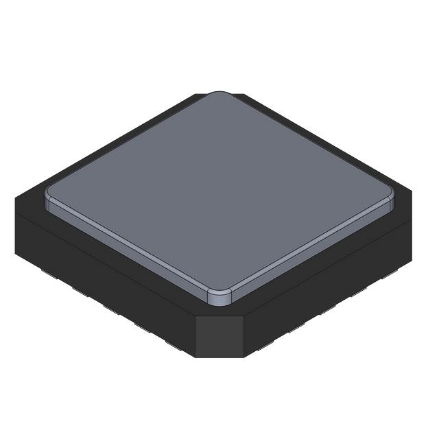
SNJ54LS242FK
Manufacturer No:
SNJ54LS242FK
Manufacturer:
Description:
BUS TRANSCEIVER, LS SERIES TTL
Datasheet:
Delivery:


Payment:


In Stock : 450
Please send RFQ , we will respond immediately.


SNJ54LS242FK Specifications
-
TypeParameter
-
Supplier Device Package-
-
Package / Case-
-
Mounting Type-
-
Operating Temperature-
-
Voltage - Supply-
-
Current - Output High, Low-
-
Output Type-
-
Input Type-
-
Logic Type-
-
PackagingBulk
-
Product StatusActive
-
Series*
The SNJ54LS242FK is a specific type of integrated circuit chip, part of the LS family from Texas Instruments. This chip is a Quad Bus Buffer with 3-State Outputs. Advantages:1. Multiple outputs: The SNJ54LS242FK has four separate buffer inputs and outputs, allowing the chip to handle multiple signals simultaneously.2. 3-state outputs: The 3-state outputs enable the chip to be in three different states: high (1), low (0), or high-impedance. The high-impedance state is useful when multiple chips are connected to a common bus, as it prevents any interference or conflicts when two or more buffers try to drive the bus simultaneously.3. Buffering capability: The chip acts as a buffer between the inputs and outputs, allowing signals to be amplified or inverted if required. It provides a stable output that can drive other circuits without being affected by the input signal's characteristics.Application scenarios:1. Bus buffering: The SNJ54LS242FK is commonly used in applications where multiple chips need to communicate with each other through a shared bus. The chip can buffer the signals to prevent interference and maintain the integrity of data transmission.2. Signal amplification: When a weak input signal needs to be amplified to drive a circuit, this chip can be used as a buffer to boost the signal's strength without significantly affecting the original signal.3. Digital logic systems: The LS family of chips, including the SNJ54LS242FK, is often used in digital systems where logic levels need to be controlled and maintained. The chip can interface between different logic families or voltage levels, ensuring compatibility and signal integrity.4. Multiplexing and demultiplexing: The quad buffer design of the SNJ54LS242FK makes it suitable for multiplexing and demultiplexing applications. It can select and route signals from multiple sources to a single output or vice versa, expanding the capabilities of a circuit.Overall, the SNJ54LS242FK integrated circuit chip offers advantages such as multiple outputs, 3-state outputs, and buffering capability. It finds applications in bus buffering, signal amplification, digital logic systems, and multiplexing/demultiplexing scenarios.
SNJ54LS242FK Relevant information
-

SN74ALVTH162245LR
Texas Instruments -
SN74BCT623NSR
Texas Instruments -
CY74FCT16543ATPACT
Texas Instruments -
SN74LVTH652DGVR
Texas Instruments -
SN74LVTH646DGVR
Texas Instruments -
SN74LVTH2952DGVR
Texas Instruments -

SN74LVTH162241DL
Texas Instruments -
SN74LVC828ADBR
Texas Instruments -

SN74ALVTH162244LR
Texas Instruments -
SN74ALVCH162344VR
Texas Instruments


