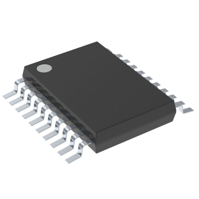
SN74LVC2G07YZAR
Manufacturer No:
SN74LVC2G07YZAR
Manufacturer:
Description:
IC BUF NON-INVERT 5.5V 6DSBGA
Datasheet:
Delivery:


Payment:


In Stock : 0
Please send RFQ , we will respond immediately.


SN74LVC2G07YZAR Specifications
-
TypeParameter
-
Supplier Device Package6-DSBGA
-
Package / Case6-XFBGA, DSBGA
-
Mounting TypeSurface Mount
-
Operating Temperature-40°C ~ 125°C (TA)
-
Voltage - Supply1.65V ~ 5.5V
-
Current - Output High, Low-, 32mA
-
Output TypeOpen Drain
-
Input Type-
-
Number of Bits per Element1
-
Number of Elements2
-
Logic TypeBuffer, Non-Inverting
-
PackagingBulk
-
PackagingCut Tape (CT)
-
PackagingTape & Reel (TR)
-
Product StatusObsolete
-
Series74LVC
The SN74LVC2G07YZAR is a dual buffer/driver integrated circuit chip manufactured by Texas Instruments. It offers several advantages and can be used in various application scenarios. Some of the advantages and application scenarios of the SN74LVC2G07YZAR are:Advantages: 1. Low power consumption: The chip operates at a low voltage and consumes minimal power, making it suitable for battery-powered devices and energy-efficient applications. 2. High-speed operation: It has a high-speed propagation delay, enabling fast data transmission and signal buffering. 3. Wide operating voltage range: The chip can operate within a wide voltage range, making it compatible with different power supply levels. 4. Small form factor: The chip is available in a small package, making it suitable for space-constrained applications and compact designs. 5. ESD protection: It provides built-in electrostatic discharge (ESD) protection, safeguarding the chip from damage due to static electricity.Application Scenarios: 1. Signal buffering: The SN74LVC2G07YZAR can be used to buffer and amplify signals in various digital systems, such as microcontrollers, FPGAs, and communication interfaces. 2. Level shifting: It can be employed for level shifting applications, where signals need to be converted from one voltage level to another, ensuring compatibility between different logic families or voltage domains. 3. Clock distribution: The chip can be used to distribute clock signals in synchronous digital systems, ensuring accurate and synchronized timing across multiple components. 4. I/O expansion: It can be utilized to expand the input/output capabilities of microcontrollers or other digital devices, enabling connection to a larger number of peripherals or sensors. 5. Bus driving: The chip can drive data buses in various applications, such as memory interfaces, data acquisition systems, or communication protocols.These are just a few examples of the advantages and application scenarios of the SN74LVC2G07YZAR. The chip's versatility, low power consumption, and small form factor make it suitable for a wide range of digital and mixed-signal applications.
SN74LVC2G07YZAR Relevant information
-

SN74ALVTH162245LR
Texas Instruments -

SN74BCT623NSR
Texas Instruments -

CY74FCT16543ATPACT
Texas Instruments -
SN74LVTH652DGVR
Texas Instruments -
SN74LVTH646DGVR
Texas Instruments -
SN74LVTH2952DGVR
Texas Instruments -

SN74LVTH162241DL
Texas Instruments -

SN74LVC828ADBR
Texas Instruments -

SN74ALVTH162244LR
Texas Instruments -

SN74ALVCH162344VR
Texas Instruments


