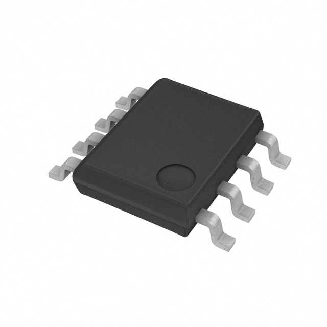
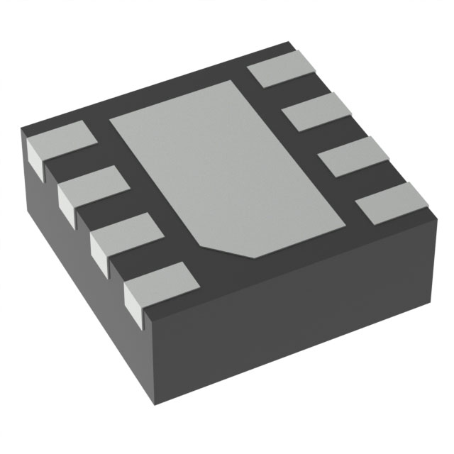
ADCMP565BP
Manufacturer No:
ADCMP565BP
Manufacturer:
Description:
IC COMPARATOR 2 W/LATCH 20PLCC
Datasheet:
Delivery:


Payment:


In Stock : 0
Please send RFQ , we will respond immediately.


ADCMP565BP Specifications
-
TypeParameter
-
Supplier Device Package20-PLCC (9x9)
-
Mounting TypeSurface Mount
-
Package / Case20-LCC (J-Lead)
-
Operating Temperature-40°C ~ 85°C
-
Hysteresis±1mV
-
Propagation Delay (Max)0.375ns
-
CMRR, PSRR (Typ)69dB CMRR
-
Current - Quiescent (Max)18mA, 80mA
-
Current - Output (Typ)30mA
-
Current - Input Bias (Max)40µA @ 5V
-
Voltage - Input Offset (Max)6mV @ 5V
-
Voltage - Supply, Single/Dual (±)±4.75V ~ 5.25V
-
Output TypeComplementary, Differential, ECL, Open-Emitter
-
Number of Elements2
-
Typewith Latch
-
PackagingTube
-
PackagingTube
-
Product StatusObsolete
-
Series-
The ADCMP565BP is a high-speed voltage comparator integrated circuit chip. It offers several advantages and can be applied in various scenarios. Some of the advantages and application scenarios of the ADCMP565BP are:Advantages: 1. High Speed: The ADCMP565BP is designed for high-speed applications, with a propagation delay of less than 1 ns. This makes it suitable for applications that require fast response times.2. Low Power Consumption: The chip operates at a low supply voltage and consumes minimal power, making it suitable for battery-powered devices or applications where power efficiency is crucial.3. Wide Input Voltage Range: The ADCMP565BP can handle a wide range of input voltages, from -0.3V to +5.5V. This flexibility allows it to be used in various voltage level detection or monitoring applications.4. Rail-to-Rail Outputs: The chip provides rail-to-rail output swing, meaning it can drive signals close to the supply voltage rails. This feature is beneficial in applications where the output needs to be compatible with other devices or circuits.Application Scenarios: 1. High-Speed Signal Processing: The ADCMP565BP can be used in high-speed signal processing applications, such as data communication systems, where fast and accurate voltage comparisons are required.2. Level Shifting and Translation: The wide input voltage range and rail-to-rail outputs make the ADCMP565BP suitable for level shifting and translation applications. It can be used to interface signals between different voltage domains or to convert signals to a compatible level for further processing.3. Window Comparators: The chip's high-speed operation and wide input voltage range make it suitable for window comparator applications. Window comparators are used to monitor if a signal falls within a specific voltage range, and the ADCMP565BP can quickly detect if the signal is within the desired window.4. Timing and Synchronization: The fast propagation delay of the ADCMP565BP makes it suitable for timing and synchronization applications. It can be used to compare the timing of different signals or synchronize events in systems where precise timing is critical.Overall, the ADCMP565BP integrated circuit chip offers high-speed, low power consumption, wide input voltage range, and rail-to-rail outputs, making it suitable for various applications requiring fast and accurate voltage comparisons.
ADCMP565BP Relevant information


