


Share

LTC6255CDC
Manufacturer No:
LTC6255CDC
Manufacturer:
Description:
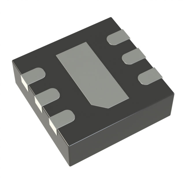
IC OPAMP GP 1 CIRCUIT 6DFN
Datasheet:
Delivery:


Payment:


In Stock : 0
Please send RFQ , we will respond immediately.


LTC6255CDC Specifications
-
TypeParameter
-
Supplier Device Package6-DFN (2x2)
-
Package / Case6-WFDFN Exposed Pad
-
Mounting TypeSurface Mount
-
Operating Temperature0°C ~ 70°C
-
Voltage - Supply Span (Max)5.25 V
-
Voltage - Supply Span (Min)1.8 V
-
Current - Output / Channel35 mA
-
Current - Supply65µA
-
Voltage - Input Offset100 µV
-
Current - Input Bias5 nA
-
-3db Bandwidth4.5 MHz
-
Gain Bandwidth Product6.5 MHz
-
Slew Rate1.8V/µs
-
Output TypeRail-to-Rail
-
Number of Circuits1
-
Amplifier TypeGeneral Purpose
-
PackagingTube
-
Product StatusObsolete
-
Series-
The LTC6255CDC is a high-speed, low-power operational amplifier (op-amp) integrated circuit chip manufactured by Linear Technology (now part of Analog Devices). It offers several advantages and finds applications in various scenarios. Some of the advantages and application scenarios of the LTC6255CDC are:Advantages: 1. High Speed: The LTC6255CDC is a high-speed op-amp with a gain bandwidth product of 180 MHz. It can handle fast signal processing requirements, making it suitable for applications that require high-speed amplification.2. Low Power Consumption: This op-amp chip operates at low power, making it suitable for battery-powered or low-power applications. It has a supply current of only 1.3 mA, which helps in reducing power consumption.3. Rail-to-Rail Inputs and Outputs: The LTC6255CDC supports rail-to-rail input and output voltage ranges. It can handle signals that swing close to the supply rails, enabling it to work with a wide range of input and output voltages.4. Low Input Bias Current: With an input bias current of only 1 pA, the LTC6255CDC is suitable for applications that require high-impedance inputs. It minimizes the impact of input bias current on the accuracy of the circuit.5. Low Input Offset Voltage: The op-amp chip has a low input offset voltage of 300 μV, which helps in achieving accurate amplification and signal processing.Application Scenarios: 1. Signal Conditioning: The LTC6255CDC can be used in signal conditioning applications where high-speed amplification and low power consumption are required. It can amplify and condition signals from sensors, transducers, or other sources before further processing.2. Data Acquisition Systems: The high-speed and low-power characteristics of the LTC6255CDC make it suitable for data acquisition systems. It can amplify and process analog signals from sensors or other sources before digitization.3. Portable Devices: Due to its low power consumption, the LTC6255CDC is well-suited for portable devices such as handheld instruments, battery-powered systems, or portable medical devices. It can provide amplification and signal processing while minimizing power drain.4. Communications: The high-speed capabilities of the LTC6255CDC make it useful in communication systems. It can be used for amplification and filtering of high-frequency signals in applications such as wireless communication, audio processing, or RF circuits.5. Test and Measurement Equipment: The LTC6255CDC can be employed in test and measurement equipment that requires high-speed amplification and accurate signal processing. It can be used in oscilloscopes, spectrum analyzers, or other measurement instruments.Overall, the LTC6255CDC offers high-speed, low-power, and versatile performance, making it suitable for a wide range of applications that require amplification and signal conditioning.
LTC6255CDC Relevant information
-
AD8034ARZ-REEL7
Analog Devices Inc. -
CA3140AMZ
Renesas Electronics America Inc -

OP07CPZ
Analog Devices Inc. -
LT1636CMS8#TRPBF
Analog Devices Inc. -
LT1490ACS8#TRPBF
Analog Devices Inc. -
LTC2055HMS8#TRPBF
Analog Devices Inc. -
AD8227BRMZ-R7
Analog Devices Inc. -
AD8227BRZ-R7
Analog Devices Inc. -
AD623ARZ-R7
Analog Devices Inc. -
AD623ARMZ-REEL7
Analog Devices Inc.