


Share

LTC6253CDC
Manufacturer No:
LTC6253CDC
Manufacturer:
Description:
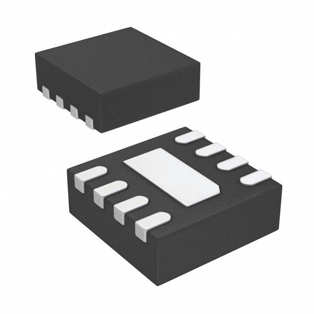
IC OPAMP GP 2 CIRCUIT 8DFN
Datasheet:
Delivery:


Payment:


In Stock : 0
Please send RFQ , we will respond immediately.


LTC6253CDC Specifications
-
TypeParameter
-
Supplier Device Package8-DFN (2x2)
-
Package / Case8-WFDFN Exposed Pad
-
Mounting TypeSurface Mount
-
Operating Temperature0°C ~ 70°C
-
Voltage - Supply Span (Max)5.25 V
-
Voltage - Supply Span (Min)2.5 V
-
Current - Output / Channel100 mA
-
Current - Supply4.25mA (x2 Channels)
-
Voltage - Input Offset100 µV
-
Current - Input Bias1.4 µA
-
-3db Bandwidth400 MHz
-
Gain Bandwidth Product720 MHz
-
Slew Rate280V/µs
-
Output TypeRail-to-Rail
-
Number of Circuits2
-
Amplifier TypeGeneral Purpose
-
PackagingTube
-
Product StatusObsolete
-
Series-
The LTC6253CDC is a low power, rail-to-rail input and output operational amplifier (op-amp) integrated circuit chip. Some of its advantages and application scenarios include:1. Low power consumption: The LTC6253CDC is designed to operate with very low power consumption, making it suitable for battery-powered applications or any application where power efficiency is crucial.2. Rail-to-rail input and output: The op-amp has rail-to-rail input and output capabilities, which means it can handle signals that swing close to the power supply rails. This feature allows for maximum utilization of the available voltage range, making it suitable for applications that require a wide dynamic range.3. High precision and accuracy: The LTC6253CDC offers high precision and accuracy in amplification and signal processing. It has low input offset voltage, low input bias current, and low input noise, making it suitable for applications that require high-quality signal amplification and conditioning.4. Wide supply voltage range: The chip can operate with a wide supply voltage range, typically from 2.7V to 5.5V. This flexibility allows it to be used in various applications with different power supply configurations.5. Small package size: The LTC6253CDC is available in small package options, such as the 6-lead DFN (Dual Flat No-Lead) package. This compact size makes it suitable for space-constrained applications or designs where miniaturization is a requirement.Application scenarios for the LTC6253CDC include:1. Portable and battery-powered devices: Due to its low power consumption and wide supply voltage range, the chip is suitable for applications like portable audio devices, handheld instruments, and battery-powered sensors.2. Sensor signal conditioning: The high precision and accuracy of the LTC6253CDC make it suitable for amplifying and conditioning signals from various sensors, such as temperature sensors, pressure sensors, or strain gauges.3. Data acquisition systems: The chip's rail-to-rail input and output capabilities, combined with its low noise characteristics, make it suitable for use in data acquisition systems where accurate and high-quality signal amplification is required.4. Industrial and automotive applications: The LTC6253CDC's wide supply voltage range and small package size make it suitable for various industrial and automotive applications, such as motor control, instrumentation, or automotive sensor interfaces.5. Portable medical devices: The low power consumption and small package size of the chip make it suitable for portable medical devices, such as glucose meters, blood pressure monitors, or wearable health trackers.
LTC6253CDC Relevant information
-
AD8034ARZ-REEL7
Analog Devices Inc. -
CA3140AMZ
Renesas Electronics America Inc -

OP07CPZ
Analog Devices Inc. -
LT1636CMS8#TRPBF
Analog Devices Inc. -
LT1490ACS8#TRPBF
Analog Devices Inc. -
LTC2055HMS8#TRPBF
Analog Devices Inc. -
AD8227BRMZ-R7
Analog Devices Inc. -
AD8227BRZ-R7
Analog Devices Inc. -
AD623ARZ-R7
Analog Devices Inc. -
AD623ARMZ-REEL7
Analog Devices Inc.