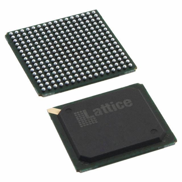
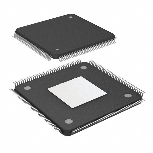
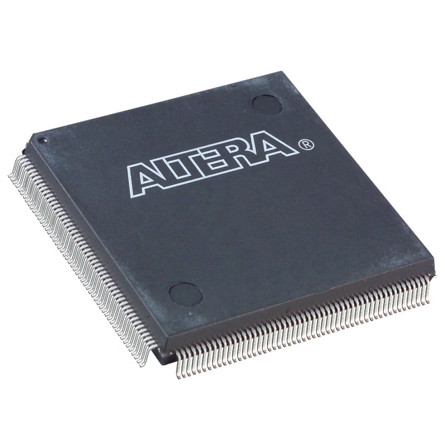
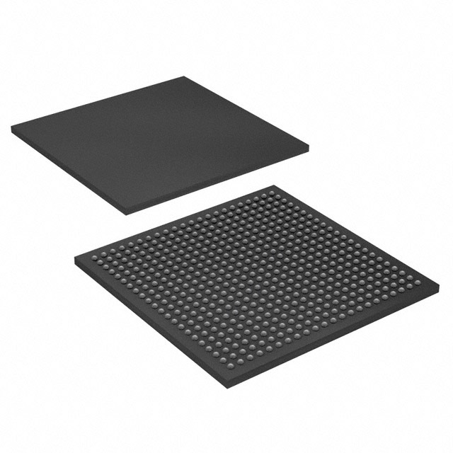
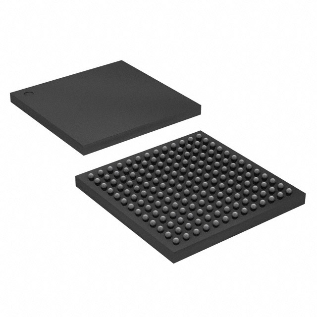
LFE2M100E-5FN900C
Manufacturer No:
LFE2M100E-5FN900C
Manufacturer:
Description:
IC FPGA 416 I/O 900FBGA
Datasheet:
Delivery:


Payment:


In Stock : 0
Please send RFQ , we will respond immediately.


LFE2M100E-5FN900C Specifications
-
TypeParameter
-
Number of Logic Elements/Cells95000
-
Number of LABs/CLBs11875
-
Supplier Device Package900-FPBGA (31x31)
-
Package / Case900-BBGA
-
Operating Temperature0°C ~ 85°C (TJ)
-
Mounting TypeSurface Mount
-
Voltage - Supply1.14V ~ 1.26V
-
Number of I/O416
-
Total RAM Bits5435392
-
DigiKey ProgrammableNot Verified
-
PackagingTray
-
Product StatusActive
-
SeriesECP2M
The LFE2M100E-5FN900C is a specific model of the Lattice Semiconductor's ECP5 FPGA (Field-Programmable Gate Array) family. This FPGA chip offers several advantages and can be used in various application scenarios. Some of the advantages and application scenarios of the LFE2M100E-5FN900C are:Advantages: 1. High Performance: The LFE2M100E-5FN900C FPGA chip provides high-performance capabilities, including high-speed data processing, low latency, and high bandwidth. It can handle complex algorithms and computations efficiently.2. Low Power Consumption: This FPGA chip is designed to be power-efficient, making it suitable for applications where power consumption is a critical factor. It allows for energy-efficient designs and extends battery life in portable devices.3. Flexibility and Reconfigurability: Being a field-programmable device, the LFE2M100E-5FN900C FPGA chip offers flexibility and reconfigurability. It can be programmed and reprogrammed to perform different functions, making it adaptable to changing requirements and reducing the need for hardware redesign.4. High Integration: The LFE2M100E-5FN900C FPGA chip integrates various components, including logic elements, memory blocks, DSP (Digital Signal Processing) slices, and I/O interfaces. This integration simplifies the overall system design, reduces component count, and saves board space.5. Security Features: The LFE2M100E-5FN900C FPGA chip provides security features like bitstream encryption and authentication, protecting the intellectual property and preventing unauthorized access or tampering.Application Scenarios: 1. Communications and Networking: The high-performance and low-latency capabilities of the LFE2M100E-5FN900C make it suitable for applications in telecommunications, networking, and data centers. It can be used for packet processing, protocol conversion, encryption/decryption, and network acceleration.2. Industrial Automation: The FPGA chip's flexibility and integration make it ideal for industrial automation applications. It can be used for real-time control, sensor interfacing, motor control, and machine vision processing.3. Video and Image Processing: The LFE2M100E-5FN900C FPGA chip's high-speed data processing and DSP capabilities make it well-suited for video and image processing applications. It can be used for video encoding/decoding, image recognition, and computer vision tasks.4. Aerospace and Defense: The FPGA chip's high-performance computing and security features make it suitable for aerospace and defense applications. It can be used in radar systems, avionics, secure communication systems, and electronic warfare.5. Internet of Things (IoT): The low power consumption and integration capabilities of the LFE2M100E-5FN900C FPGA chip make it suitable for IoT applications. It can be used for sensor data processing, edge computing, and IoT gateway devices.These are just a few examples of the advantages and application scenarios of the LFE2M100E-5FN900C FPGA chip. Its versatility and performance make it applicable in various industries and domains where high-performance, low-power, and flexible computing solutions are required.


