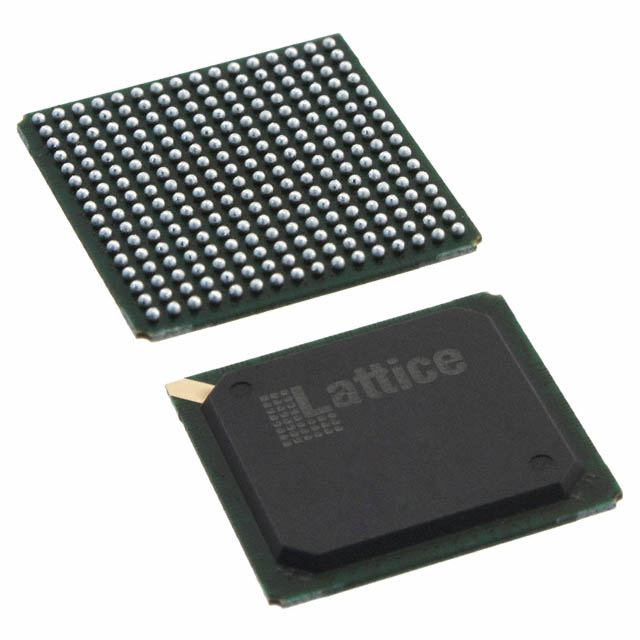
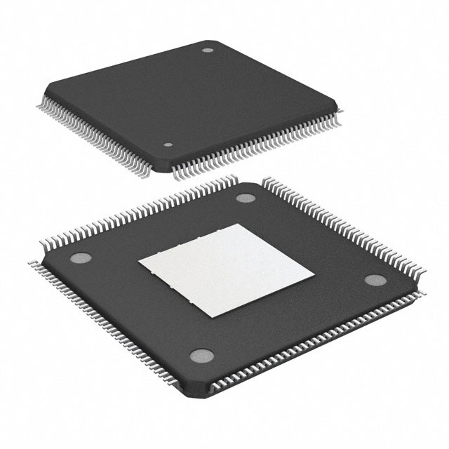
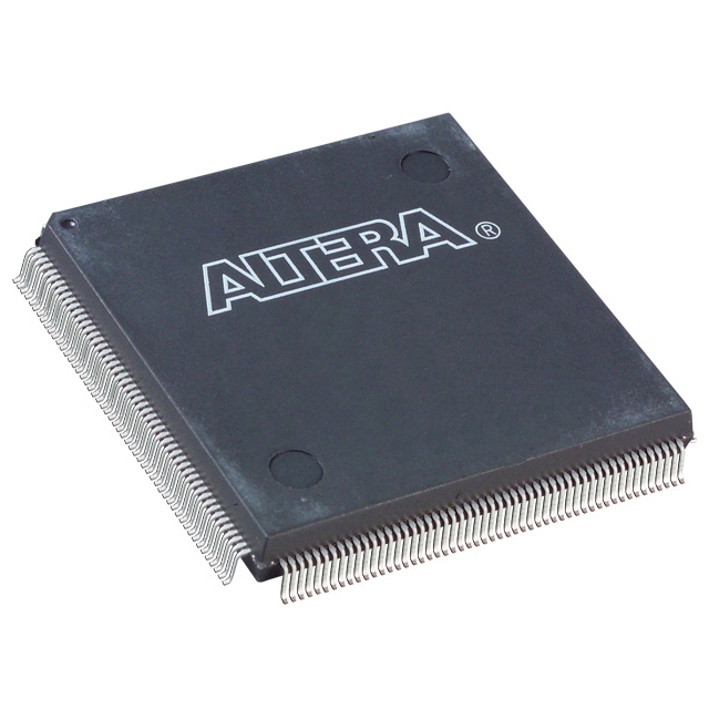
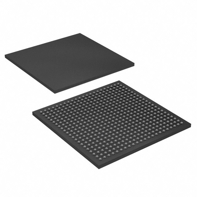
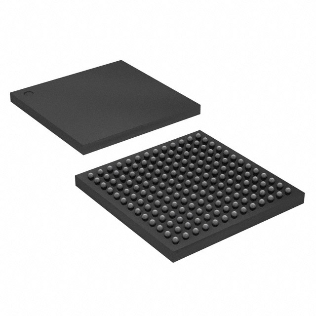
ICE40HX8K-CT256
Manufacturer No:
ICE40HX8K-CT256
Manufacturer:
Description:
IC FPGA 206 I/O 256CABGA
Datasheet:
Delivery:


Payment:


In Stock : 641
Please send RFQ , we will respond immediately.


ICE40HX8K-CT256 Specifications
-
TypeParameter
-
Total RAM Bits131072
-
Supplier Device Package256-CABGA (14x14)
-
Package / Case256-LFBGA
-
Operating Temperature-40°C ~ 100°C (TJ)
-
Mounting TypeSurface Mount
-
Voltage - Supply1.14V ~ 1.26V
-
Number of I/O206
-
Number of Logic Elements/Cells7680
-
Number of LABs/CLBs960
-
DigiKey ProgrammableNot Verified
-
PackagingTray
-
Product StatusActive
-
SeriesiCE40™ HX
The ICE40HX8K-CT256 is an integrated circuit chip from the ICE40 family of FPGAs (Field-Programmable Gate Arrays) developed by Lattice Semiconductor. Here are some advantages and application scenarios of this particular chip:Advantages: 1. Low power consumption: The ICE40HX8K-CT256 is designed to be power-efficient, making it suitable for battery-powered devices or applications where power consumption is a concern. 2. Small form factor: The chip comes in a compact CT256 package, which makes it suitable for space-constrained designs or applications where size is a critical factor. 3. High logic density: With 8,000 logic cells, the ICE40HX8K-CT256 offers a relatively high logic density, allowing for the implementation of complex digital designs. 4. Flexible I/O options: The chip provides a range of I/O options, including LVCMOS, LVTTL, and differential I/O standards, enabling easy interfacing with various external devices.Application Scenarios: 1. IoT Devices: The low power consumption and small form factor of the ICE40HX8K-CT256 make it suitable for IoT (Internet of Things) devices, where power efficiency and compact size are crucial. 2. Sensor Interfaces: The chip's flexible I/O options make it well-suited for interfacing with different types of sensors, such as temperature sensors, accelerometers, or environmental sensors. 3. Consumer Electronics: The ICE40HX8K-CT256 can be used in various consumer electronic devices, including wearables, smart home devices, or portable gadgets, where power efficiency and small size are desirable. 4. Prototyping and Development: The FPGA nature of the chip allows for reprogrammability, making it ideal for prototyping and development of digital designs, such as custom logic circuits or digital signal processing algorithms.It's important to note that the specific application scenarios may vary depending on the requirements and constraints of the project.


