


Share

MC68L11E1FNE2
Manufacturer No:
MC68L11E1FNE2
Manufacturer:
Description:
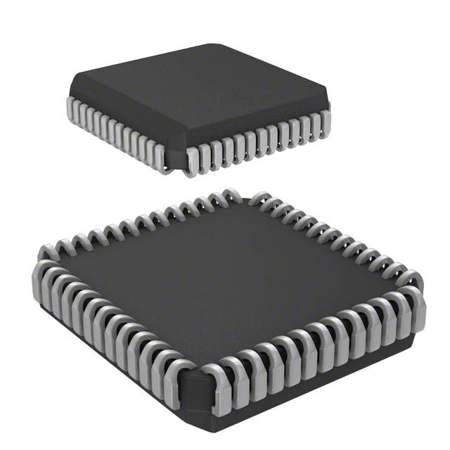
IC MCU 8BIT ROMLESS 52PLCC
Datasheet:
Delivery:


Payment:


In Stock : 0
Please send RFQ , we will respond immediately.


MC68L11E1FNE2 Specifications
-
TypeParameter
-
Supplier Device Package52-PLCC (19.1x19.1)
-
Package / Case52-LCC (J-Lead)
-
Mounting TypeSurface Mount
-
Operating Temperature0°C ~ 70°C (TA)
-
Oscillator TypeInternal
-
Data ConvertersA/D 8x8b
-
Voltage - Supply (Vcc/Vdd)3V ~ 5.5V
-
RAM Size512 x 8
-
EEPROM Size512 x 8
-
Program Memory TypeROMless
-
Program Memory Size-
-
Number of I/O38
-
PeripheralsPOR, WDT
-
ConnectivitySCI, SPI
-
Speed2MHz
-
Core Size8-Bit
-
Core ProcessorHC11
-
DigiKey ProgrammableNot Verified
-
PackagingTube
-
Product StatusObsolete
-
SeriesHC11
The ADG409BNZ is a quad CMOS analog multiplexer/demultiplexer integrated circuit chip. It offers several advantages and can be used in various application scenarios. Some of the advantages and application scenarios of the ADG409BNZ are:Advantages: 1. Low power consumption: The ADG409BNZ operates at very low power levels, making it suitable for battery-powered devices and applications where power efficiency is crucial. 2. Wide voltage range: It can handle a wide range of supply voltages, typically from ±4.5V to ±18V, allowing it to be used in diverse electronic systems. 3. Low on-resistance: The chip has low on-resistance, ensuring minimal signal distortion and accurate switching performance. 4. High switching speed: The ADG409BNZ has a fast switching speed, enabling it to handle high-frequency signals and time-critical applications. 5. Low leakage current: It exhibits low leakage current, ensuring minimal signal loss and accurate signal routing.Application Scenarios: 1. Analog signal routing: The ADG409BNZ can be used to switch and route analog signals in various applications, such as audio/video signal routing, instrumentation, and communication systems. 2. Data acquisition systems: It can be employed in data acquisition systems to multiplex multiple analog input signals and route them to a single analog-to-digital converter (ADC) for processing. 3. Test and measurement equipment: The chip can be utilized in test and measurement equipment, such as oscilloscopes and data loggers, to switch between different input signals for analysis and measurement purposes. 4. Industrial automation: The ADG409BNZ can be integrated into industrial automation systems to control and route analog signals in real-time, facilitating process control and monitoring. 5. Medical devices: It can be used in medical devices, such as patient monitoring systems and diagnostic equipment, to switch between different sensor inputs and route signals for analysis and diagnosis.These are just a few examples of the advantages and application scenarios of the ADG409BNZ integrated circuit chip. Its versatility, low power consumption, and accurate signal routing capabilities make it suitable for a wide range of analog signal switching applications.
MC68L11E1FNE2 Relevant information
-

LM3S8538-IQC50-A2
Texas Instruments -
LM3S1937-IQC50-A2
Texas Instruments -
LM3S1637-IQC50-A2
Texas Instruments -
LM3S1635-IQC50-A2
Texas Instruments -
LM3S1332-IQC50-A2
Texas Instruments -
LM3S1165-IQC50-A2
Texas Instruments -
LM3S1162-IQC50-A2
Texas Instruments -
LM3S1133-IQC50-A2
Texas Instruments -
LM3S308-IQN25
Texas Instruments -
P89LPC936FA,529
NXP USA Inc.