


Share
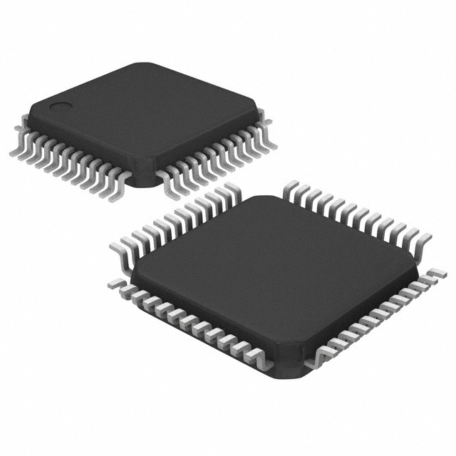

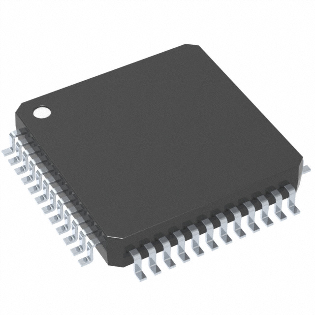
R5F10PGGCKFB#35
Manufacturer No:
R5F10PGGCKFB#35
Manufacturer:
Description:
IC MCU 16BIT 128KB FLASH 48LFQFP
Datasheet:
Delivery:


Payment:


In Stock : 0
Please send RFQ , we will respond immediately.


R5F10PGGCKFB#35 Specifications
-
TypeParameter
-
Supplier Device Package48-LFQFP (7x7)
-
Package / Case48-LQFP
-
Mounting TypeSurface Mount
-
Operating Temperature-40°C ~ 125°C (TA)
-
Oscillator TypeInternal
-
Data ConvertersA/D 17x10b SAR; D/A 1x8b
-
Voltage - Supply (Vcc/Vdd)2.7V ~ 5.5V
-
RAM Size10K x 8
-
EEPROM Size8K x 8
-
Program Memory TypeFLASH
-
Program Memory Size128KB (128K x 8)
-
Number of I/O38
-
PeripheralsLVD, POR, PWM, WDT
-
ConnectivityCANbus, CSI, I²C, LINbus, SPI, UART/USART
-
Speed24MHz
-
Core Size16-Bit
-
Core ProcessorRL78
-
DigiKey ProgrammableNot Verified
-
PackagingTray
-
Product StatusActive
-
SeriesRL78/F14
The 74LVC1G53DP,125 is a dual 2-input multiplexer integrated circuit chip. It has several advantages and application scenarios, including:1. Small package size: The chip comes in a small SOT353 package, making it suitable for applications with limited space or where miniaturization is required.2. Low power consumption: The 74LVC1G53DP,125 operates at low power supply voltages (1.65V to 5.5V) and has low power dissipation, making it ideal for battery-powered devices or applications where power efficiency is crucial.3. High-speed operation: The chip has a high-speed switching capability, with propagation delays as low as 3.5 ns. This makes it suitable for applications that require fast data switching or multiplexing.4. Wide operating temperature range: The chip can operate in a wide temperature range (-40°C to 125°C), making it suitable for both commercial and industrial applications.5. ESD protection: The 74LVC1G53DP,125 provides ESD protection up to 2 kV, ensuring robustness against electrostatic discharge events.Application scenarios for the 74LVC1G53DP,125 include:1. Data multiplexing: The chip can be used to select between two different data sources and route the selected data to an output. This is useful in applications such as data switches, signal routing, or data selection in digital systems.2. Logic level conversion: The chip can be used to convert logic levels between different voltage domains. For example, it can interface between a microcontroller operating at 3.3V and a peripheral device operating at 5V.3. Signal routing and selection: The chip can be used to route or select different signals in various applications, such as audio/video switching, communication systems, or test and measurement equipment.4. Battery-powered devices: The low power consumption and wide operating voltage range of the chip make it suitable for battery-powered devices, such as portable electronics, wearables, or IoT devices.5. Industrial automation: The chip's robustness, wide temperature range, and small package size make it suitable for industrial automation applications, such as sensor interfacing, control systems, or PLCs (Programmable Logic Controllers).Overall, the 74LVC1G53DP,125 integrated circuit chip offers advantages in terms of size, power consumption, speed, and temperature range, making it suitable for a wide range of applications requiring data multiplexing, logic level conversion, signal routing, or selection.
R5F10PGGCKFB#35 Relevant information
-

LM3S8538-IQC50-A2
Texas Instruments -
LM3S1937-IQC50-A2
Texas Instruments -
LM3S1637-IQC50-A2
Texas Instruments -
LM3S1635-IQC50-A2
Texas Instruments -
LM3S1332-IQC50-A2
Texas Instruments -
LM3S1165-IQC50-A2
Texas Instruments -
LM3S1162-IQC50-A2
Texas Instruments -
LM3S1133-IQC50-A2
Texas Instruments -
LM3S308-IQN25
Texas Instruments -
P89LPC936FA,529
NXP USA Inc.