


Share
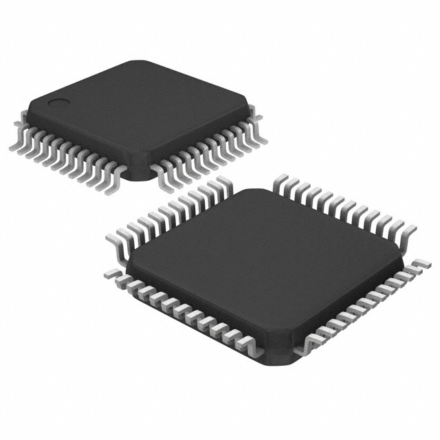

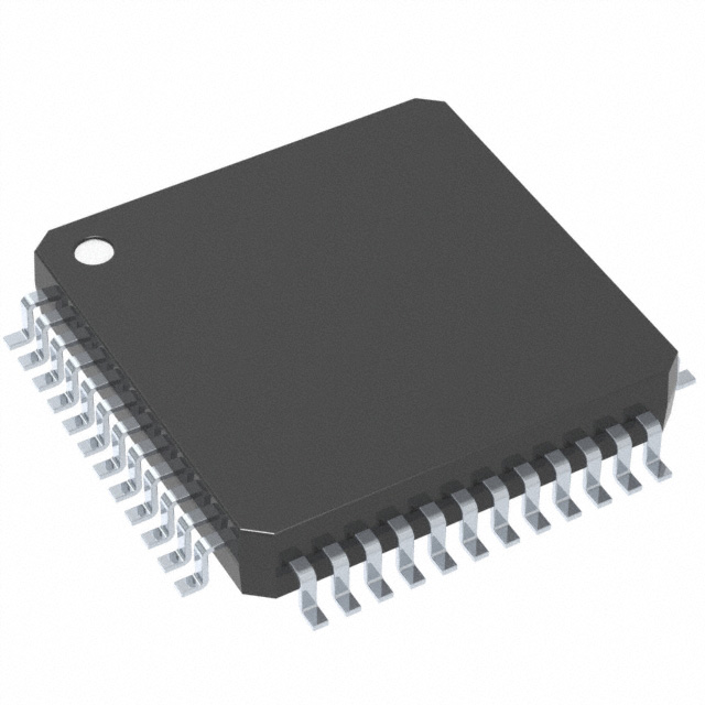
R5F10DGDCJFB#32G
Manufacturer No:
R5F10DGDCJFB#32G
Manufacturer:
Description:
IC MCU 16BIT 48KB FLASH 48LFQFP
Datasheet:
Delivery:


Payment:


In Stock : 0
Please send RFQ , we will respond immediately.


R5F10DGDCJFB#32G Specifications
-
TypeParameter
-
Supplier Device Package48-LFQFP (7x7)
-
Package / Case48-LQFP
-
Mounting TypeSurface Mount
-
Operating Temperature-40°C ~ 85°C (TA)
-
Oscillator TypeInternal
-
Data ConvertersA/D 5x10b
-
Voltage - Supply (Vcc/Vdd)2.7V ~ 5.5V
-
RAM Size3K x 8
-
EEPROM Size8K x 8
-
Program Memory TypeFLASH
-
Program Memory Size48KB (48K x 8)
-
Number of I/O35
-
PeripheralsDMA, Motor Control, LCD, LVD, POR, PWM, WDT
-
ConnectivityCANbus, CSI, I²C, LINbus, UART/USART
-
Speed32MHz
-
Core Size16-Bit
-
Core ProcessorRL78
-
DigiKey ProgrammableNot Verified
-
PackagingTray
-
Product StatusActive
-
SeriesRL78/D1x
The 74LVC2G66GM is a dual bilateral switch integrated circuit chip. It offers several advantages and can be used in various application scenarios. Some of the advantages and application scenarios of the 74LVC2G66GM are:Advantages: 1. Low power consumption: The chip operates at low power supply voltage, making it suitable for battery-powered devices and energy-efficient applications. 2. Wide operating voltage range: It can operate within a wide voltage range, allowing compatibility with different power supply levels. 3. Fast switching speed: The chip has a high-speed switching capability, enabling quick signal routing and transmission. 4. Low propagation delay: It has a low propagation delay, ensuring minimal signal delay during switching operations. 5. Low input/output capacitance: The chip has low input and output capacitance, reducing the loading effect on the connected circuitry.Application Scenarios: 1. Signal routing and switching: The 74LVC2G66GM can be used to route and switch analog or digital signals in various applications, such as audio/video systems, communication devices, and test equipment. 2. Level shifting: It can be employed for level shifting applications, where signals need to be converted from one voltage level to another, ensuring compatibility between different circuitry. 3. Multiplexing: The chip can be used for multiplexing applications, where multiple signals are combined and transmitted over a single channel. 4. Input/output expansion: It can be utilized to expand the number of input/output ports in microcontrollers or other digital devices, enabling connectivity with a larger number of external devices. 5. Logic level conversion: The chip can be used to convert logic levels between different voltage standards, facilitating communication between devices operating at different voltage levels.These are just a few examples of the advantages and application scenarios of the 74LVC2G66GM integrated circuit chip. Its versatility and features make it suitable for a wide range of electronic applications.
R5F10DGDCJFB#32G Relevant information
-

LM3S8538-IQC50-A2
Texas Instruments -
LM3S1937-IQC50-A2
Texas Instruments -
LM3S1637-IQC50-A2
Texas Instruments -
LM3S1635-IQC50-A2
Texas Instruments -
LM3S1332-IQC50-A2
Texas Instruments -
LM3S1165-IQC50-A2
Texas Instruments -
LM3S1162-IQC50-A2
Texas Instruments -
LM3S1133-IQC50-A2
Texas Instruments -
LM3S308-IQN25
Texas Instruments -
P89LPC936FA,529
NXP USA Inc.