


Share

DF61523RJ48FPQVAD8
Manufacturer No:
DF61523RJ48FPQVAD8
Manufacturer:
Description:
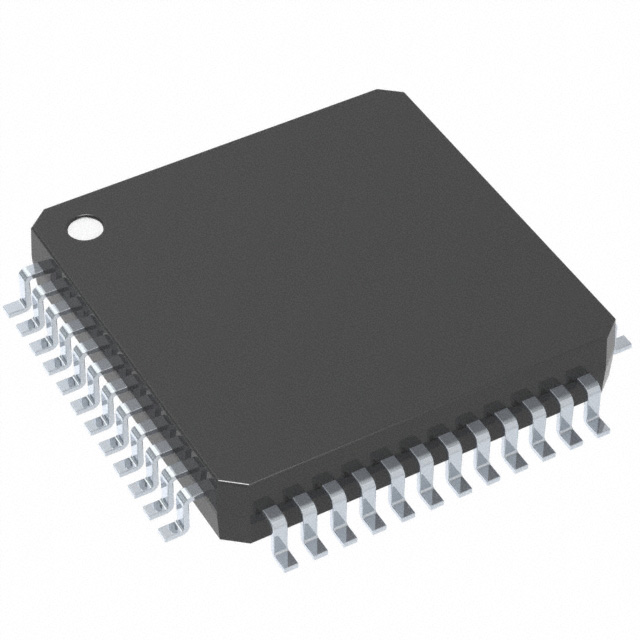
IC MCU 32BIT CORE SMD
Datasheet:
Delivery:


Payment:


In Stock : 0
Please send RFQ , we will respond immediately.


DF61523RJ48FPQVAD8 Specifications
-
TypeParameter
-
Supplier Device Package-
-
Package / Case-
-
Mounting Type-
-
Operating Temperature-
-
Oscillator Type-
-
Data Converters-
-
Voltage - Supply (Vcc/Vdd)-
-
RAM Size-
-
EEPROM Size-
-
Program Memory Type-
-
Program Memory Size-
-
Peripherals-
-
Connectivity-
-
Speed-
-
Core Size-
-
Core Processor-
-
DigiKey ProgrammableNot Verified
-
PackagingTape & Reel (TR)
-
Product StatusObsolete
-
Series-
The SN74LVC2G53DCUTG4 is a dual 2-input multiplexer integrated circuit chip. It offers several advantages and can be used in various application scenarios. Some of the advantages and application scenarios of this chip are:Advantages: 1. Low power consumption: The SN74LVC2G53DCUTG4 operates at a low voltage and consumes minimal power, making it suitable for battery-powered devices and energy-efficient applications. 2. High-speed operation: It has a high-speed switching capability, enabling it to handle fast data rates and time-critical applications. 3. Wide operating voltage range: The chip can operate within a wide voltage range, making it compatible with different power supply levels. 4. Small form factor: The SN74LVC2G53DCUTG4 is available in a small package, making it suitable for space-constrained designs and compact electronic devices. 5. ESD protection: It provides built-in electrostatic discharge (ESD) protection, safeguarding the chip from damage due to static electricity.Application Scenarios: 1. Data multiplexing: The SN74LVC2G53DCUTG4 can be used to select between two different data sources and route the selected data to an output. It is commonly used in data communication systems, such as multiplexing different data streams onto a single transmission line. 2. Signal routing: It can be used to switch between different input signals and route them to different output paths. This is useful in applications where multiple signals need to be selectively routed, such as audio/video switchers or signal routing matrices. 3. Logic level conversion: The chip can be used to convert logic levels between different voltage domains. It enables interfacing between devices operating at different voltage levels, ensuring compatibility and seamless communication. 4. Control signal selection: It can be used to select between different control signals and route the selected signal to a specific control input. This is useful in applications where different control signals need to be selectively applied, such as in microcontrollers or digital systems. 5. Redundancy switching: The SN74LVC2G53DCUTG4 can be used to implement redundancy switching, where two redundant components or signals are monitored, and the chip automatically switches to the backup component/signal in case of failure or error.These are just a few examples of the advantages and application scenarios of the SN74LVC2G53DCUTG4 integrated circuit chip. Its versatility, low power consumption, and small form factor make it suitable for a wide range of electronic designs and applications.
DF61523RJ48FPQVAD8 Relevant information
-

LM3S8538-IQC50-A2
Texas Instruments -
LM3S1937-IQC50-A2
Texas Instruments -
LM3S1637-IQC50-A2
Texas Instruments -
LM3S1635-IQC50-A2
Texas Instruments -
LM3S1332-IQC50-A2
Texas Instruments -
LM3S1165-IQC50-A2
Texas Instruments -
LM3S1162-IQC50-A2
Texas Instruments -
LM3S1133-IQC50-A2
Texas Instruments -
LM3S308-IQN25
Texas Instruments -
P89LPC936FA,529
NXP USA Inc.