


Share

R5F562N7BNLE#U0
Manufacturer No:
R5F562N7BNLE#U0
Manufacturer:
Description:
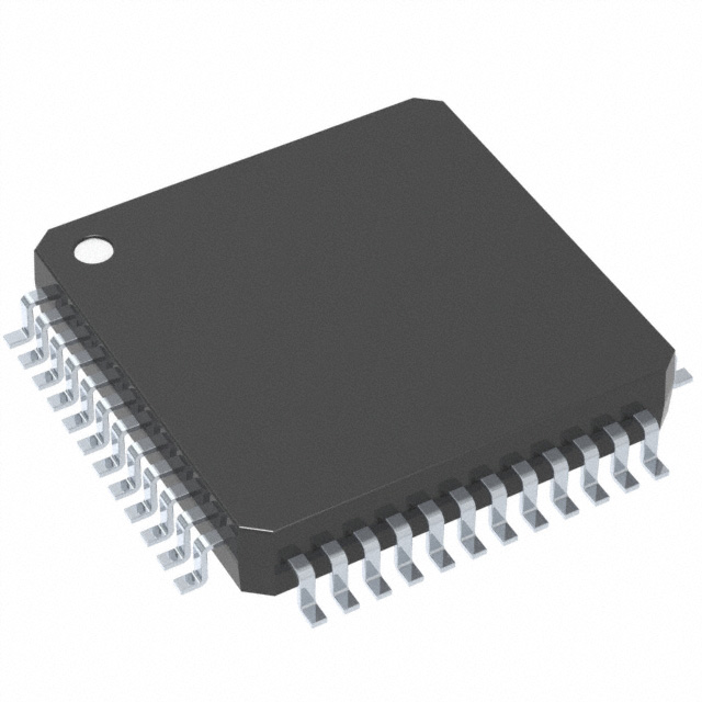
IC MCU 32BIT 384KB FLASH 145LGA
Datasheet:
Delivery:


Payment:


In Stock : 0
Please send RFQ , we will respond immediately.


R5F562N7BNLE#U0 Specifications
-
TypeParameter
-
Supplier Device Package-
-
Package / Case-
-
Mounting Type-
-
Operating Temperature-
-
Oscillator Type-
-
Data Converters-
-
Voltage - Supply (Vcc/Vdd)-
-
RAM Size-
-
EEPROM Size-
-
Program Memory Type-
-
Program Memory Size-
-
Peripherals-
-
Connectivity-
-
Speed-
-
Core Size-
-
Core Processor-
-
DigiKey ProgrammableNot Verified
-
PackagingTape & Reel (TR)
-
Product StatusObsolete
-
Series-
The NX3L4051PW-Q100J is a high-performance integrated circuit chip that belongs to the NX3L series of analog multiplexers/demultiplexers. Here are some advantages and application scenarios of this chip:Advantages: 1. Low power consumption: The chip operates at a low supply voltage range of 1.1V to 3.6V, making it suitable for battery-powered devices and low-power applications. 2. Wide voltage range: It supports a wide voltage range of 1.65V to 5.5V, allowing compatibility with various digital and analog systems. 3. Low on-resistance: The chip offers low on-resistance, resulting in minimal signal distortion and improved signal integrity. 4. High bandwidth: It provides a high bandwidth, enabling the transmission of high-frequency signals without significant loss or degradation. 5. ESD protection: The chip incorporates built-in electrostatic discharge (ESD) protection, safeguarding the device from potential damage due to static electricity.Application scenarios: 1. Analog signal multiplexing: The NX3L4051PW-Q100J chip can be used to select and route analog signals from multiple sources to a single output, making it suitable for applications such as audio/video signal switching, data acquisition systems, and instrumentation. 2. Digital signal multiplexing: It can also be used for digital signal multiplexing, allowing multiple digital signals to be routed to a single output, which is useful in applications like digital communication systems, data transmission, and digital signal processing. 3. Signal routing and switching: The chip can be employed for general-purpose signal routing and switching tasks, where multiple input signals need to be selectively connected to different output channels. 4. Test and measurement equipment: Due to its high performance and low power consumption, the chip finds applications in test and measurement equipment, where accurate signal routing and switching are required. 5. Portable devices: The low power consumption and wide voltage range make the chip suitable for portable devices such as smartphones, tablets, and wearable devices, where power efficiency and compatibility with different voltage levels are crucial.Overall, the NX3L4051PW-Q100J integrated circuit chip offers advantages like low power consumption, wide voltage range, and high performance, making it suitable for various analog and digital signal routing applications in different industries.
R5F562N7BNLE#U0 Relevant information
-

LM3S8538-IQC50-A2
Texas Instruments -
LM3S1937-IQC50-A2
Texas Instruments -
LM3S1637-IQC50-A2
Texas Instruments -
LM3S1635-IQC50-A2
Texas Instruments -
LM3S1332-IQC50-A2
Texas Instruments -
LM3S1165-IQC50-A2
Texas Instruments -
LM3S1162-IQC50-A2
Texas Instruments -
LM3S1133-IQC50-A2
Texas Instruments -
LM3S308-IQN25
Texas Instruments -
P89LPC936FA,529
NXP USA Inc.