


Share

R5F1017AANA#W0
Manufacturer No:
R5F1017AANA#W0
Manufacturer:
Description:
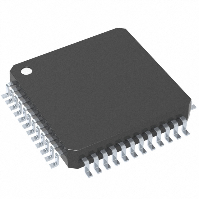
IC MCU 16BIT 16KB FLASH 24HWQFN
Datasheet:
Delivery:


Payment:


In Stock : 0
Please send RFQ , we will respond immediately.


R5F1017AANA#W0 Specifications
-
TypeParameter
-
Supplier Device Package24-HWQFN (4x4)
-
Package / Case24-WFQFN Exposed Pad
-
Mounting TypeSurface Mount
-
Operating Temperature-40°C ~ 85°C (TA)
-
Oscillator TypeInternal
-
Data ConvertersA/D 6x8/10b
-
Voltage - Supply (Vcc/Vdd)1.6V ~ 5.5V
-
RAM Size2K x 8
-
EEPROM Size-
-
Program Memory TypeFLASH
-
Program Memory Size16KB (16K x 8)
-
Number of I/O15
-
PeripheralsDMA, LVD, POR, PWM, WDT
-
ConnectivityCSI, I²C, UART/USART
-
Speed32MHz
-
Core Size16-Bit
-
Core ProcessorRL78
-
DigiKey ProgrammableNot Verified
-
PackagingTape & Reel (TR)
-
Product StatusObsolete
-
SeriesRL78/G13
The NC7SB3157P6X-F40 is a specific integrated circuit chip that belongs to the NC7 series of high-performance CMOS logic gates. It is a single-pole, double-throw (SPDT) analog switch, which means it can connect one input to either of two outputs. Here are some advantages and application scenarios of this chip:Advantages: 1. Low power consumption: The NC7SB3157P6X-F40 operates at very low power levels, making it suitable for battery-powered devices and other low-power applications. 2. Wide operating voltage range: It can operate within a wide voltage range, typically from 1.65V to 5.5V, making it compatible with various voltage levels. 3. Fast switching speed: The chip has a fast propagation delay, enabling quick switching between inputs and outputs. 4. Low on-resistance: It has low on-resistance, resulting in minimal signal distortion and attenuation.Application scenarios: 1. Audio and video signal routing: The NC7SB3157P6X-F40 can be used in audio and video systems to switch between different input sources or route signals to different output devices. 2. Communication systems: It can be employed in communication systems to switch between different antennas or channels, allowing for signal selection and routing. 3. Test and measurement equipment: The chip can be used in test and measurement devices to switch between different test points or signal paths, facilitating signal analysis and troubleshooting. 4. Portable devices: Due to its low power consumption and small form factor, the chip is suitable for use in portable devices such as smartphones, tablets, and wearable technology, where space and power efficiency are crucial.It is important to note that the specific application scenarios may vary depending on the requirements of the system and the capabilities of the chip. It is recommended to consult the datasheet and application notes provided by the manufacturer for detailed information and guidelines on using the NC7SB3157P6X-F40 chip.
R5F1017AANA#W0 Relevant information
-

LM3S8538-IQC50-A2
Texas Instruments -
LM3S1937-IQC50-A2
Texas Instruments -
LM3S1637-IQC50-A2
Texas Instruments -
LM3S1635-IQC50-A2
Texas Instruments -
LM3S1332-IQC50-A2
Texas Instruments -
LM3S1165-IQC50-A2
Texas Instruments -
LM3S1162-IQC50-A2
Texas Instruments -
LM3S1133-IQC50-A2
Texas Instruments -
LM3S308-IQN25
Texas Instruments -
P89LPC936FA,529
NXP USA Inc.