


Share

R5F104GHGNA#U0
Manufacturer No:
R5F104GHGNA#U0
Manufacturer:
Description:
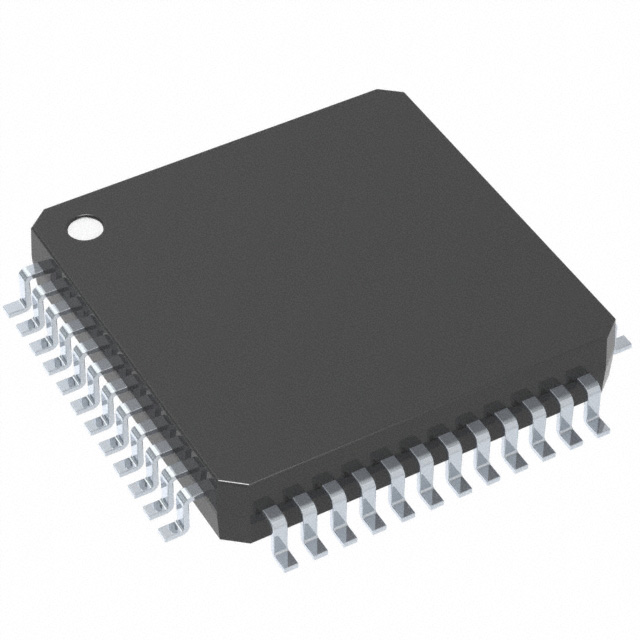
IC MCU 16BIT 192KB FLASH 48HWQFN
Datasheet:
Delivery:


Payment:


In Stock : 0
Please send RFQ , we will respond immediately.


R5F104GHGNA#U0 Specifications
-
TypeParameter
-
Supplier Device Package48-HWQFN (7x7)
-
Package / Case48-WFQFN Exposed Pad
-
Mounting TypeSurface Mount
-
Operating Temperature-40°C ~ 105°C (TA)
-
Oscillator TypeInternal
-
Data ConvertersA/D 10x8/10b; D/A 2x8b
-
Voltage - Supply (Vcc/Vdd)2.4V ~ 5.5V
-
RAM Size20K x 8
-
EEPROM Size8K x 8
-
Program Memory TypeFLASH
-
Program Memory Size192KB (192K x 8)
-
Number of I/O34
-
PeripheralsDMA, LVD, POR, PWM, WDT
-
ConnectivityCSI, I²C, LINbus, UART/USART
-
Speed32MHz
-
Core Size16-Bit
-
Core ProcessorRL78
-
DigiKey ProgrammableNot Verified
-
PackagingTray
-
Product StatusObsolete
-
SeriesRL78/G14
The CD4052BD3 is a dual 4-channel analog multiplexer/demultiplexer integrated circuit chip. It has several advantages and application scenarios, including:1. Versatility: The CD4052BD3 can be used as a multiplexer or demultiplexer, allowing for flexible signal routing and switching. It can handle both analog and digital signals.2. Low power consumption: The chip operates at a low power supply voltage (typically 3-15V) and has low power dissipation, making it suitable for battery-powered devices and low-power applications.3. High speed: The CD4052BD3 has a fast switching speed, allowing for rapid signal routing and switching. This makes it suitable for applications that require quick response times.4. Wide operating temperature range: The chip can operate in a wide temperature range (-55°C to 125°C), making it suitable for use in harsh environments.5. Small form factor: The CD4052BD3 is available in a compact package, making it suitable for space-constrained applications.Some application scenarios where the CD4052BD3 can be used include:1. Audio and video signal routing: The chip can be used to switch between different audio or video sources, such as selecting different inputs for a speaker system or switching between different video sources in a surveillance system.2. Data acquisition systems: The CD4052BD3 can be used to multiplex multiple analog signals into a single analog-to-digital converter (ADC), reducing the number of ADCs required in a data acquisition system.3. Instrumentation and measurement systems: The chip can be used to route different sensor signals to a measurement device, allowing for multiplexing of multiple sensors.4. Communication systems: The CD4052BD3 can be used in communication systems to switch between different channels or to route signals to different components, such as antennas or transceivers.5. Industrial control systems: The chip can be used in industrial control systems to route different control signals to different actuators or devices, allowing for flexible control and automation.Overall, the CD4052BD3 offers versatility, low power consumption, high speed, and a wide operating temperature range, making it suitable for a variety of applications that require signal routing and switching.
R5F104GHGNA#U0 Relevant information
-

LM3S8538-IQC50-A2
Texas Instruments -
LM3S1937-IQC50-A2
Texas Instruments -
LM3S1637-IQC50-A2
Texas Instruments -
LM3S1635-IQC50-A2
Texas Instruments -
LM3S1332-IQC50-A2
Texas Instruments -
LM3S1165-IQC50-A2
Texas Instruments -
LM3S1162-IQC50-A2
Texas Instruments -
LM3S1133-IQC50-A2
Texas Instruments -
LM3S308-IQN25
Texas Instruments -
P89LPC936FA,529
NXP USA Inc.