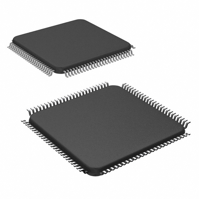
SCANSTA112VS/NOPB
Manufacturer No:
SCANSTA112VS/NOPB
Manufacturer:
Description:
IC INTERFACE SPECIALIZED 100TQFP
Datasheet:
Delivery:


Payment:


In Stock : 0
Please send RFQ , we will respond immediately.


SCANSTA112VS/NOPB Specifications
-
TypeParameter
-
Mounting TypeSurface Mount
-
Supplier Device Package100-TQFP (14x14)
-
Package / Case100-TQFP
-
Voltage - Supply3V ~ 3.6V
-
InterfaceIEEE 1149.1
-
ApplicationsTesting Equipment
-
PackagingTray
-
PackagingBulk
-
Product StatusNot For New Designs
-
Series-
The SCANSTA112VS/NOPB is a highly integrated circuit chip designed for scan-based testing and debugging of digital systems. It offers several advantages and can be applied in various scenarios. Here are some of the advantages and application scenarios of the SCANSTA112VS/NOPB:Advantages: 1. High Integration: The SCANSTA112VS/NOPB integrates multiple scan test and debug functions into a single chip, reducing the need for external components and simplifying the testing process. 2. Flexibility: It supports various scan test modes, including boundary scan, internal scan, and memory BIST, providing flexibility in testing different types of digital systems. 3. Fast Test Speed: The chip is designed for high-speed testing, enabling quick and efficient testing of digital systems, thereby reducing overall testing time. 4. Debugging Capabilities: It offers advanced debugging features like scan-based emulation and observability, allowing engineers to identify and resolve issues in the digital system. 5. Low Power Consumption: The SCANSTA112VS/NOPB is designed to operate at low power, ensuring minimal impact on the power consumption of the tested digital system.Application Scenarios: 1. Semiconductor Manufacturing: The chip is widely used in semiconductor manufacturing for testing and debugging digital systems, ensuring the quality and reliability of the manufactured chips. 2. PCB Testing: It can be applied in printed circuit board (PCB) testing to verify the functionality and integrity of digital components on the board. 3. System Integration: The SCANSTA112VS/NOPB can be used during the integration of various digital components into a larger system, ensuring proper connectivity and functionality. 4. Product Development: It is commonly used during the development phase of digital products to validate the design and identify any potential issues or bugs. 5. Field Testing and Maintenance: The chip can be utilized in field testing and maintenance of digital systems, allowing engineers to diagnose and fix problems in deployed systems.Overall, the SCANSTA112VS/NOPB integrated circuit chip offers a range of advantages and can be applied in various scenarios to facilitate efficient and reliable testing and debugging of digital systems.
SCANSTA112VS/NOPB Relevant information
-
TLE92623QXV33XUMA1
Analog Devices Inc. -
TDA8034HN/C1,118
Analog Devices Inc. -
UJA1076ATW/5V0WD,1
Analog Devices Inc. -
MC33797BPEW
Infineon Technologies -
SP7611AEC6-L
National Semiconductor -
PTN3365BSMP
ams-OSRAM USA INC. -
PTN3393BS/F1Y
ams-OSRAM USA INC. -
PCA9541AD/01,112
National Semiconductor -
MC33889BPEG
onsemi -
TLE92623QXV33XUMA1
Analog Devices Inc.


