


Share

MAX368EWN
Manufacturer No:
MAX368EWN
Manufacturer:
Description:
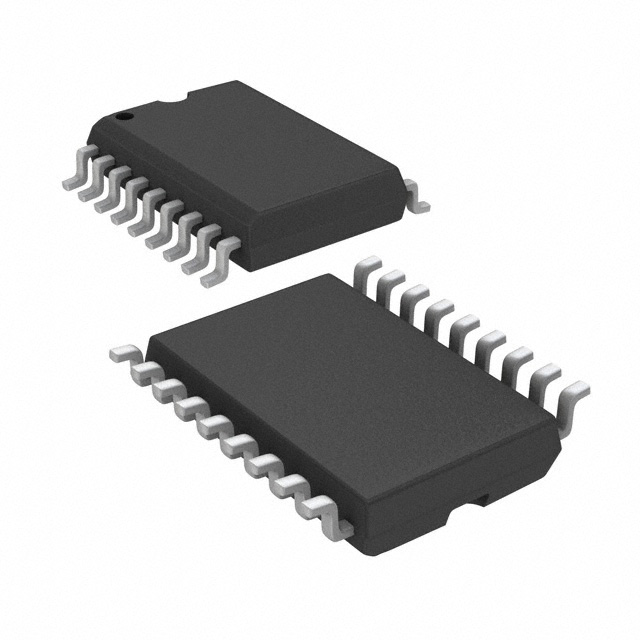
IC MUX 8:1 1.8KOHM 18SOIC
Datasheet:
Delivery:


Payment:


In Stock : 0
Please send RFQ , we will respond immediately.


MAX368EWN Specifications
-
TypeParameter
-
Supplier Device Package18-SOIC
-
Package / Case18-SOIC (0.295", 7.50mm Width)
-
Mounting TypeSurface Mount
-
Operating Temperature-40°C ~ 85°C (TA)
-
Crosstalk-
-
Current - Leakage (IS(off)) (Max)5nA
-
Channel Capacitance (CS(off), CD(off))5pF, 25pF
-
Charge Injection55pC
-
-3db Bandwidth-
-
Switch Time (Ton, Toff) (Max)1.5µs, 1µs
-
Voltage - Supply, Dual (V±)±4.5V ~ 18V
-
Voltage - Supply, Single (V+)-
-
Channel-to-Channel Matching (ΔRon)180Ohm
-
On-State Resistance (Max)1.8kOhm
-
Number of Circuits1
-
Multiplexer/Demultiplexer Circuit8:1
-
Switch Circuit-
-
PackagingTube
-
Product StatusObsolete
-
Series-
The M2S150-1FCV484 is an integrated circuit chip manufactured by Microsemi Corporation. It belongs to the SmartFusion2 family of system-on-chip (SoC) devices. Here are some advantages and application scenarios of the M2S150-1FCV484:Advantages: 1. Versatility: The M2S150-1FCV484 is a highly versatile chip that combines an FPGA (Field-Programmable Gate Array) fabric with a hard ARM Cortex-M3 microcontroller subsystem. This combination allows for flexible hardware customization and software programmability, making it suitable for a wide range of applications. 2. Integration: The chip integrates various components, including FPGA fabric, microcontroller subsystem, memory, and peripherals, onto a single chip. This integration reduces the need for external components, simplifies the design, and saves board space. 3. Security: The SmartFusion2 family, including the M2S150-1FCV484, offers advanced security features such as secure boot, tamper detection, and secure key storage. These features make it suitable for applications that require high levels of security, such as industrial control systems, defense, and aerospace. 4. Low power consumption: The M2S150-1FCV484 is designed to be power-efficient, making it suitable for battery-powered or energy-constrained applications. It incorporates power management features to optimize power consumption and extend battery life.Application scenarios: 1. Industrial automation: The M2S150-1FCV484 can be used in industrial automation systems for tasks such as motor control, sensor interfacing, and communication protocols. Its FPGA fabric allows for customization and adaptation to specific industrial requirements. 2. Internet of Things (IoT): With its combination of FPGA and microcontroller subsystem, the chip is well-suited for IoT applications. It can handle sensor data processing, communication protocols, and security features required in IoT devices. 3. Aerospace and defense: The M2S150-1FCV484's security features, low power consumption, and integration make it suitable for aerospace and defense applications. It can be used in avionics systems, secure communication systems, and military-grade equipment. 4. Medical devices: The chip's versatility and security features make it suitable for medical devices that require customization, data processing, and secure operation. It can be used in devices such as patient monitors, diagnostic equipment, and implantable devices.These are just a few examples of the advantages and application scenarios of the M2S150-1FCV484. The chip's flexibility and integration make it applicable to a wide range of industries and use cases.
MAX368EWN Relevant information
-
DG509AAZ/883B
Analog Devices Inc./Maxim Integrated -
TS12A4514PE4
Analog Devices Inc. -
TS3A24159DGSR
Analog Devices Inc. -
TS12A4515DBVR
Analog Devices Inc. -
SW202NBC
NXP Semiconductors -
MAX464CNI
NXP Semiconductors -
MC74HC4051ADWR2G
NXP Semiconductors -
74LVC1G3157GWXL
Nexperia USA Inc. -
SW202NBC
NXP Semiconductors -
TDA3683J/N2S,112
Analog Devices Inc.