


Share

MAX4634ETB
Manufacturer No:
MAX4634ETB
Manufacturer:
Description:
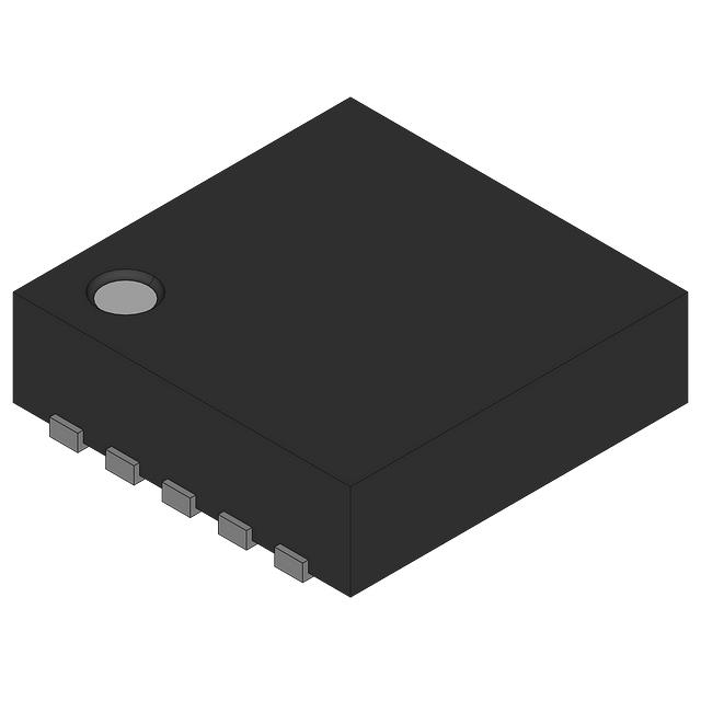
IC SWITCH SP4T X 1 4OHM 10TDFN
Datasheet:
Delivery:


Payment:


In Stock : 1744
Please send RFQ , we will respond immediately.


MAX4634ETB Specifications
-
TypeParameter
-
Supplier Device Package10-TDFN-EP (3x3)
-
Package / Case10-WFDFN Exposed Pad
-
Mounting TypeSurface Mount
-
Operating Temperature-40°C ~ 85°C (TA)
-
Crosstalk-52dB @ 10MHz
-
Current - Leakage (IS(off)) (Max)100pA
-
Channel Capacitance (CS(off), CD(off))13pF
-
Charge Injection2pC
-
-3db Bandwidth-
-
Switch Time (Ton, Toff) (Max)18ns, 11ns
-
Voltage - Supply, Dual (V±)-
-
Voltage - Supply, Single (V+)1.8V ~ 5.5V
-
Channel-to-Channel Matching (ΔRon)100mOhm
-
On-State Resistance (Max)4Ohm
-
Number of Circuits1
-
Multiplexer/Demultiplexer Circuit4:1
-
Switch CircuitSP4T
-
PackagingBulk
-
Product StatusActive
-
Series-
The M2S150-1FCS536 is an integrated circuit chip developed by Microsemi Corporation. It belongs to the SmartFusion2 family of system-on-chip (SoC) devices. Here are some advantages and application scenarios of this chip:Advantages: 1. Versatility: The M2S150-1FCS536 chip combines an FPGA (Field-Programmable Gate Array) fabric with a hard ARM Cortex-M3 microcontroller subsystem. This combination allows for flexible hardware customization and software programmability, making it suitable for a wide range of applications. 2. Integration: The chip integrates various components, including FPGA fabric, microcontroller subsystem, memory, and peripherals, onto a single chip. This integration reduces the need for external components, simplifies the design, and saves board space. 3. Security: The SmartFusion2 family incorporates security features such as secure boot, tamper detection, and secure key storage. This makes the M2S150-1FCS536 chip suitable for applications that require robust security measures. 4. Low power consumption: The chip is designed to operate with low power consumption, making it suitable for battery-powered or energy-efficient applications. 5. High performance: The FPGA fabric and ARM Cortex-M3 microcontroller subsystem provide high-performance processing capabilities, enabling the chip to handle complex tasks and applications.Application scenarios: 1. Industrial automation: The M2S150-1FCS536 chip can be used in industrial automation systems for tasks such as motor control, sensor interfacing, and communication protocols. The FPGA fabric allows for customization and adaptation to specific industrial requirements. 2. Internet of Things (IoT): With its low power consumption and integration of FPGA and microcontroller, the chip can be used in IoT devices for edge computing, data processing, and connectivity. 3. Aerospace and defense: The security features of the SmartFusion2 family make the M2S150-1FCS536 chip suitable for aerospace and defense applications that require secure boot, data protection, and tamper detection. 4. Medical devices: The chip's versatility and integration make it suitable for medical devices such as patient monitoring systems, medical imaging equipment, and diagnostic devices. 5. Communications: The M2S150-1FCS536 chip can be used in communication systems for tasks such as protocol conversion, signal processing, and encryption/decryption.These are just a few examples of the advantages and application scenarios of the M2S150-1FCS536 chip. The versatility and integration of this chip make it suitable for a wide range of applications where both hardware customization and software programmability are required.
MAX4634ETB Relevant information
-
DG509AAZ/883B
Analog Devices Inc./Maxim Integrated -
TS12A4514PE4
Analog Devices Inc. -
TS3A24159DGSR
Analog Devices Inc. -
TS12A4515DBVR
Analog Devices Inc. -
SW202NBC
NXP Semiconductors -
MAX464CNI
NXP Semiconductors -
MC74HC4051ADWR2G
NXP Semiconductors -
74LVC1G3157GWXL
Nexperia USA Inc. -
SW202NBC
NXP Semiconductors -
TDA3683J/N2S,112
Analog Devices Inc.