


Share

MAX337CAI+T
Manufacturer No:
MAX337CAI+T
Manufacturer:
Description:
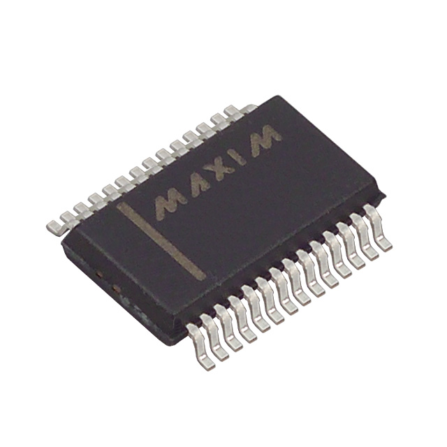
IC MUX DUAL 8:1 400OHM 28SSOP
Datasheet:
Delivery:


Payment:


In Stock : 0
Please send RFQ , we will respond immediately.


MAX337CAI+T Specifications
-
TypeParameter
-
Supplier Device Package28-SSOP
-
Package / Case28-SSOP (0.209", 5.30mm Width)
-
Mounting TypeSurface Mount
-
Operating Temperature0°C ~ 70°C (TA)
-
Crosstalk-86dB @ 100kHz
-
Current - Leakage (IS(off)) (Max)20pA
-
Channel Capacitance (CS(off), CD(off))2pF, 20pF
-
Charge Injection3.5pC
-
-3db Bandwidth-
-
Switch Time (Ton, Toff) (Max)500ns, 500ns
-
Voltage - Supply, Dual (V±)±4.5V ~ 20V
-
Voltage - Supply, Single (V+)4.5V ~ 20V
-
Channel-to-Channel Matching (ΔRon)5Ohm
-
On-State Resistance (Max)400Ohm
-
Number of Circuits2
-
Multiplexer/Demultiplexer Circuit8:1
-
Switch Circuit-
-
PackagingTape & Reel (TR)
-
Product StatusActive
-
Series-
The A2F500M3G-1FGG256I is an integrated circuit chip from Microsemi Corporation. It belongs to the SmartFusion2 family of system-on-chip (SoC) devices. Here are some advantages and application scenarios of this chip:Advantages: 1. Versatility: The A2F500M3G-1FGG256I chip combines an FPGA (Field-Programmable Gate Array) with a microcontroller subsystem, providing the benefits of both technologies in a single device. This versatility allows for a wide range of applications.2. Integration: The chip integrates various components, including FPGA fabric, ARM Cortex-M3 processor, programmable analog, and digital peripherals. This integration reduces the need for external components, simplifying the design and reducing the overall system cost.3. Security: The SmartFusion2 family emphasizes security features, including secure boot, tamper detection, and data encryption. These features make the A2F500M3G-1FGG256I suitable for applications that require robust security measures.4. Low power consumption: The chip is designed to be power-efficient, making it suitable for battery-powered or energy-conscious applications.Application Scenarios: 1. Industrial Automation: The A2F500M3G-1FGG256I chip can be used in industrial automation systems, such as programmable logic controllers (PLCs), where the FPGA fabric can be utilized for real-time control and the microcontroller subsystem can handle communication protocols and other tasks.2. Internet of Things (IoT): With its integrated microcontroller and FPGA capabilities, the chip can be used in IoT applications that require both processing power and programmable logic. It can be employed in smart home devices, sensor networks, or edge computing systems.3. Aerospace and Defense: The security features of the SmartFusion2 family make the A2F500M3G-1FGG256I suitable for aerospace and defense applications. It can be used in avionics systems, secure communication devices, or military-grade embedded systems.4. Medical Devices: The chip's low power consumption and integration of analog peripherals make it suitable for medical devices. It can be used in patient monitoring systems, portable medical devices, or diagnostic equipment.5. Automotive: The A2F500M3G-1FGG256I chip can be employed in automotive applications, such as advanced driver-assistance systems (ADAS), infotainment systems, or vehicle control units, where the FPGA fabric can be utilized for real-time processing and the microcontroller subsystem can handle communication and control tasks.It's important to note that the specific application scenarios may vary depending on the requirements and customization of the chip within a particular system.
MAX337CAI+T Relevant information
-
DG509AAZ/883B
Analog Devices Inc./Maxim Integrated -
TS12A4514PE4
Analog Devices Inc. -
TS3A24159DGSR
Analog Devices Inc. -
TS12A4515DBVR
Analog Devices Inc. -
SW202NBC
NXP Semiconductors -
MAX464CNI
NXP Semiconductors -
MC74HC4051ADWR2G
NXP Semiconductors -
74LVC1G3157GWXL
Nexperia USA Inc. -
SW202NBC
NXP Semiconductors -
TDA3683J/N2S,112
Analog Devices Inc.