


Share
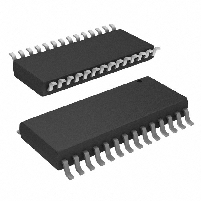

MAX306EWI+T
Manufacturer No:
MAX306EWI+T
Manufacturer:
Description:
IC MUX 16:1 100OHM 28SOIC
Datasheet:
Delivery:


Payment:


In Stock : 0
Please send RFQ , we will respond immediately.


MAX306EWI+T Specifications
-
TypeParameter
-
Supplier Device Package28-SOIC
-
Package / Case28-SOIC (0.295", 7.50mm Width)
-
Mounting TypeSurface Mount
-
Operating Temperature-40°C ~ 85°C (TA)
-
Crosstalk-92dB @ 100kHz
-
Current - Leakage (IS(off)) (Max)500pA
-
Channel Capacitance (CS(off), CD(off))8pF, 130pF
-
Charge Injection2pC
-
-3db Bandwidth-
-
Switch Time (Ton, Toff) (Max)200ns, 150ns
-
Voltage - Supply, Dual (V±)±4.5V ~ 20V
-
Voltage - Supply, Single (V+)5V ~ 30V
-
Channel-to-Channel Matching (ΔRon)1.5Ohm
-
On-State Resistance (Max)100Ohm
-
Number of Circuits1
-
Multiplexer/Demultiplexer Circuit16:1
-
Switch Circuit-
-
PackagingCut Tape (CT)
-
PackagingTape & Reel (TR)
-
Product StatusActive
-
Series-
The M2S150T-FCV484 is an integrated circuit chip manufactured by Microsemi Corporation. It belongs to the SmartFusion2 family of system-on-chip (SoC) devices. Here are some advantages and application scenarios of this chip:Advantages: 1. Versatility: The M2S150T-FCV484 chip combines an FPGA (Field-Programmable Gate Array) fabric with a hard ARM Cortex-M3 processor core. This combination allows for flexible hardware customization and software programmability, making it suitable for a wide range of applications. 2. Integration: The chip integrates various components, including FPGA fabric, processor, memory, and peripherals, onto a single chip. This integration reduces the need for external components, simplifies the design, and saves board space. 3. Security: The SmartFusion2 family of chips, including the M2S150T-FCV484, provides robust security features such as secure boot, tamper detection, and secure key storage. These features make it suitable for applications that require high levels of security. 4. Low power consumption: The chip is designed to operate with low power consumption, making it suitable for battery-powered or energy-efficient applications. 5. High performance: The FPGA fabric combined with the ARM Cortex-M3 processor core provides high-performance computing capabilities, enabling complex algorithms and real-time processing.Application scenarios: 1. Industrial automation: The M2S150T-FCV484 chip can be used in industrial automation applications such as programmable logic controllers (PLCs), motor control systems, and industrial networking. Its versatility allows for customization and adaptation to specific industrial requirements. 2. Aerospace and defense: The chip's security features make it suitable for aerospace and defense applications that require secure communication, encryption, and protection against tampering. 3. Medical devices: The chip's low power consumption and integration capabilities make it suitable for medical devices such as patient monitoring systems, portable medical equipment, and medical imaging devices. 4. Internet of Things (IoT): The chip's combination of FPGA and processor allows for IoT applications that require both hardware acceleration and software programmability. It can be used in IoT gateways, edge computing devices, and sensor nodes. 5. Communications: The chip can be used in communication systems such as routers, switches, and network appliances. Its high-performance computing capabilities and integration features enable efficient data processing and networking functions.These are just a few examples of the advantages and application scenarios of the M2S150T-FCV484 chip. Its versatility and integration make it suitable for a wide range of applications in various industries.
MAX306EWI+T Relevant information
-
DG509AAZ/883B
Analog Devices Inc./Maxim Integrated -
TS12A4514PE4
Analog Devices Inc. -
TS3A24159DGSR
Analog Devices Inc. -
TS12A4515DBVR
Analog Devices Inc. -
SW202NBC
NXP Semiconductors -
MAX464CNI
NXP Semiconductors -
MC74HC4051ADWR2G
NXP Semiconductors -
74LVC1G3157GWXL
Nexperia USA Inc. -
SW202NBC
NXP Semiconductors -
TDA3683J/N2S,112
Analog Devices Inc.