


Share

LTC1851CFW#PBF
Manufacturer No:
LTC1851CFW#PBF
Manufacturer:
Description:
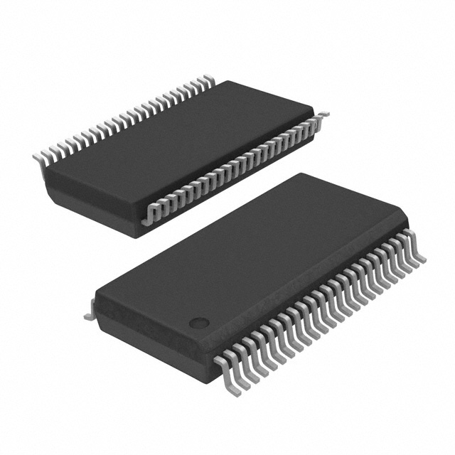
IC ADC 12BIT SAR 48TSSOP
Datasheet:
Delivery:


Payment:


In Stock : 0
Please send RFQ , we will respond immediately.


LTC1851CFW#PBF Specifications
-
TypeParameter
-
Mounting TypeSurface Mount
-
Supplier Device Package48-TSSOP
-
Package / Case48-TFSOP (0.240", 6.10mm Width)
-
Operating Temperature0°C ~ 70°C
-
FeaturesSelectable Address
-
Voltage - Supply, Digital5V
-
Voltage - Supply, Analog5V
-
Reference TypeExternal, Internal
-
ArchitectureSAR
-
Number of A/D Converters1
-
Ratio - S/H:ADC1:1
-
ConfigurationMUX-S/H-ADC
-
Data InterfaceParallel
-
Input TypeDifferential, Single Ended
-
Number of Inputs8
-
Sampling Rate (Per Second)1.25M
-
Number of Bits12
-
PackagingTube
-
Product StatusActive
-
Series-
The LTC1851CFW#PBF is a high-speed, low-power, 8-bit analog-to-digital converter (ADC) integrated circuit chip manufactured by Linear Technology (now part of Analog Devices). Some of the advantages and application scenarios of this chip are as follows:Advantages: 1. High-Speed Conversion: The LTC1851CFW#PBF is capable of converting analog signals into digital data at a high speed of up to 100 MSPS (Mega Samples Per Second). This makes it suitable for applications that require fast and real-time data acquisition.2. Low Power Consumption: The chip is designed to operate at low power, making it suitable for battery-powered or energy-efficient applications. It has a power dissipation of only 90 mW, which helps in reducing overall power consumption.3. Wide Input Bandwidth: The LTC1851CFW#PBF has a wide input bandwidth of 400 MHz, allowing it to accurately capture high-frequency signals. This makes it suitable for applications that involve high-frequency data acquisition, such as wireless communication systems or radar systems.4. Flexible Input Range: The chip supports a wide input voltage range of 1 Vpp to 2 Vpp, which can be adjusted using an external reference voltage. This flexibility allows it to handle a variety of input signal amplitudes, making it suitable for different types of sensors or signal sources.Application Scenarios: 1. Communications Systems: The high-speed and wide input bandwidth of the LTC1851CFW#PBF make it suitable for applications in communication systems, such as software-defined radios (SDR), base stations, or wireless transceivers. It can be used for signal processing, modulation/demodulation, or data acquisition in these systems.2. Test and Measurement Equipment: The chip's high-speed conversion capability and low power consumption make it suitable for use in test and measurement equipment, such as oscilloscopes, spectrum analyzers, or data loggers. It can accurately capture and digitize analog signals for further analysis or storage.3. Medical Imaging: The LTC1851CFW#PBF can be used in medical imaging applications, such as ultrasound machines or magnetic resonance imaging (MRI) systems. Its high-speed conversion and wide input bandwidth enable it to capture and process the analog signals from the imaging sensors.4. Industrial Automation: The chip can be used in industrial automation applications, such as control systems or data acquisition systems. It can convert analog sensor signals into digital data for further processing or control purposes.Overall, the LTC1851CFW#PBF integrated circuit chip offers high-speed, low-power, and accurate analog-to-digital conversion, making it suitable for various applications that require fast and precise data acquisition.
LTC1851CFW#PBF Relevant information
-
TLV5592ED
Analog Devices Inc. -
TLV1508IDWG4
Analog Devices Inc. -
ICL7136RCPL-4
Analog Devices Inc./Maxim Integrated -
LTC1415ISW#PBF
Renesas -
LTC1199LCS8#PBF
Nexperia USA Inc. -
MAX136CQH
Anadigics -
MAX1171CDJ
Infineon Technologies -
LTC1276BCSW#PBF
Nexperia USA Inc. -
ADC0831CCN
National Semiconductor -
ADC124S021CIMM
National Semiconductor