


Share

LTC3672BEDC-2#TRMPBF
Manufacturer No:
LTC3672BEDC-2#TRMPBF
Manufacturer:
Description:
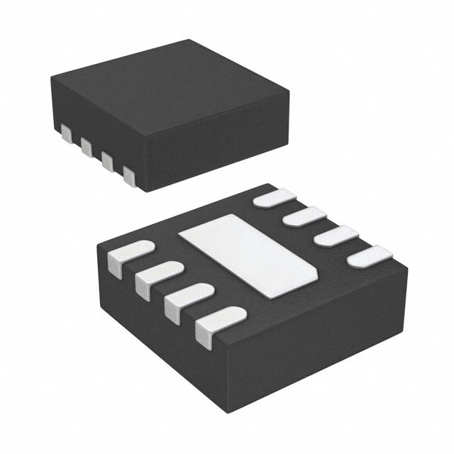
IC REG TRIPLE BUCK/LNR SYNC 8DFN
Datasheet:
Delivery:


Payment:


In Stock : 500
Please send RFQ , we will respond immediately.


LTC3672BEDC-2#TRMPBF Specifications
-
TypeParameter
-
Supplier Device Package8-DFN (2x2)
-
Package / Case8-WFDFN Exposed Pad
-
Mounting TypeSurface Mount
-
Operating Temperature-40°C ~ 85°C
-
Voltage - Supply2.9V ~ 5.5V
-
w/SequencerNo
-
w/SupervisorNo
-
w/LED DriverNo
-
Voltage/Current - Output 31.8V, 150mA
-
Voltage/Current - Output 22.8V, 150mA
-
Voltage/Current - Output 11.2V, 400mA
-
Frequency - Switching2.25MHz
-
Number of Outputs3
-
TopologyStep-Down (Buck) Synchronous (1), Linear (LDO) (2)
-
PackagingCut Tape (CT)
-
PackagingTape & Reel (TR)
-
Product StatusActive
-
Series-
The LTC3672BEDC-2#TRMPBF is a highly integrated power management IC (PMIC) chip designed by Linear Technology (now part of Analog Devices). It offers several advantages and can be applied in various scenarios. Here are some of its advantages and application scenarios:Advantages: 1. High Integration: The LTC3672BEDC-2#TRMPBF integrates multiple power management functions into a single chip, including multiple voltage regulators, a power path controller, a battery charger, and a power-on reset circuit. This high level of integration reduces the need for external components, saves board space, and simplifies the overall system design.2. Wide Input Voltage Range: The chip can operate from a wide input voltage range of 2.7V to 5.5V, making it suitable for a variety of applications and power sources.3. Flexible Power Sequencing: The LTC3672BEDC-2#TRMPBF provides flexible power sequencing options, allowing designers to control the power-up and power-down sequence of different voltage rails. This feature is particularly useful in applications where multiple power domains need to be powered up or down in a specific order to ensure proper functionality and avoid potential issues.4. Battery Charging Functionality: The chip includes a battery charger circuit that supports various battery chemistries, such as Li-Ion, Li-Polymer, and LiFePO4. It provides a constant-current/constant-voltage charging profile and includes safety features like thermal regulation and charge termination.Application Scenarios: 1. Portable Devices: The LTC3672BEDC-2#TRMPBF is well-suited for portable devices like smartphones, tablets, and handheld instruments. Its compact size, high integration, and battery charging capabilities make it ideal for powering and managing the various voltage rails required in these devices.2. IoT Devices: With the increasing popularity of Internet of Things (IoT) devices, the LTC3672BEDC-2#TRMPBF can be used to power and manage the power requirements of IoT nodes, sensors, and edge devices. Its wide input voltage range and power sequencing capabilities make it suitable for a range of IoT applications.3. Wearable Electronics: Wearable devices, such as smartwatches and fitness trackers, often have limited space for power management components. The LTC3672BEDC-2#TRMPBF's high integration and small form factor make it an excellent choice for powering and managing the various power domains in wearable electronics.4. Industrial and Automotive Applications: The chip's wide input voltage range, robustness, and power sequencing capabilities make it suitable for industrial and automotive applications. It can power and manage multiple voltage rails required in these applications, ensuring proper power-up and power-down sequencing for reliable operation.Overall, the LTC3672BEDC-2#TRMPBF offers advantages like high integration, wide input voltage range, flexible power sequencing, and battery charging functionality, making it a versatile choice for various applications requiring efficient power management.
LTC3672BEDC-2#TRMPBF Relevant information
-

TC1313-ZS0EUN
Microchip Technology -
TC1313-ZP0EUNTR
Microchip Technology -
TC1313-ZP0EUN
Microchip Technology -
TC1313-ZI0EUNTR
Microchip Technology -
TC1313-ZI0EUN
Microchip Technology -
TC1313-ZA0EUNTR
Microchip Technology -
TC1313-ZA0EUN
Microchip Technology -
TC1313-1P0EUNTR
Microchip Technology -
TC1313-1P0EUN
Microchip Technology -
TC1313-1H0EUNTR
Microchip Technology